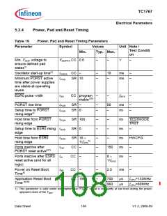
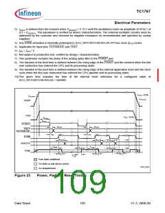
TC1767
Electrical Parameters
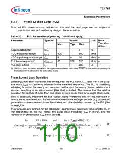
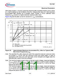
With rising number m of clock cycles the maximum jitter increases linearly up to a value
of m that is defined by the K2-factor of the PLL. Beyond this value of m the maximum
accumulated jitter remains at a constant value. Further, a lower LMB-Bus clock
frequency fLMB results in a higher absolute maximum jitter value.
Figure 26 gives the jitter curves for several K2 / fLMB combinations.
±10.0
Dm
ns
fLMB = 40 MHz (K2 = 10)
fLMB = 40 MHz (K2 = 20)
±8.0
±7.0
±6.0
±4.0
fLMB = 80 MHz (K2 = 6)
fLMB = 80 MHz (K2 = 10)
±2.0
±1.0
±0.0
fLMB = 133 MHz (K2 = 6)
20 40 60
= Max. jitter
0
80
100
120
oo
m
Dm
m
= Number of consecutive fLMB periods
K2
= K2-divider of PLL
TC1767_PLL_JITT_C
Figure 26
Approximated Maximum Accumulated PLL Jitter for Typical LMB-
Bus Clock Frequencies fLMB
Note: The specified PLL jitter values are valid if the capacitive load per output pin does
not exceed CL = 20 pF with the maximum driver and sharp edge. In case of
applications with many pins with high loads, driver strengths and toggle rates the
specified jitter values could be exceeded.
Note: The maximum peak-to-peak noise on the pad supply voltage, measured between
V
V
DDOSC3 at pin 106 and VSSOSC at pin 104, is limited to a peak-to-peak voltage of
PP = 100 mV for noise frequencies below 300 KHz and VPP = 40 mV for noise
frequencies above 300 KHz.
The maximum peak-to peak noise on the pad supply votage, measured between
VDDOSC at pin 105 and VSSOSC at pin 104, is limited to a peak-to-peak voltage of
V
PP = 100 mV for noise frequencies below 300 KHz and VPP = 40 mV for noise
frequencies above 300 KHz.
Data Sheet
107
V1.3, 2009-09

 INFINEON [ Infineon ]