TC1767
Electrical Parameters
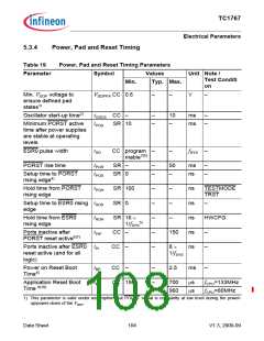
2) tOSCS is defined from the moment when VDDOSC3 = 3.13 V until the oscillations reach an amplitude at XTAL1 of
0,3 × VDDOSC3. This parameter is verified by device characterization. The external oscillator circuitry must be
optimized by the customer and checked for negative resistance as recommended and specified by crystal
suppliers.
3) Any ESR0 activation is internally prolonged to SCU_RSTCNTCON.RELSA FPI bus clock (fFPI) cycles.
4) Applicable for input pins TESTMODE and TRST.
5) fFPI = fCPU / 2
6) Not subject to production test, verified by design / characterization.
7) This parameter includes the delay of the analog spike filter in the PORST pad.
8) The duration of the boot-time is defined between the rising edge of the PORST and the moment when the first
user instruction has entered the CPU and its processing starts.
9) The duration of the boot time is defined between the rising edge of the internal application reset and the clock
cycle when the first user instruction has entered the CPU pipeline and its processing starts.
10) The given time includes the time of the internal reset extension for a configured value of
SCU_RSTCNTCON.RELSA = 0x05BE.
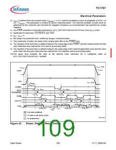
VDDP -12%
VDDPPA
VDDPPA
VDDP
VDD
VDD -12%
t
POA
t
POA
PORST
t
t
POH
POH
TRST
TESTMODE
t
t
hd
hd
ESR0
t
t
HDH
t
t
HDH
HDH
PI
HWCFG
t
t
PIP
PIP
t
PI
Pads
t
t
t
PI
PI
PI
t
PIP
Pad-state undefined
Tri-state or pull device active
As programmed
reset_beh2
Figure 25
Power, Pad and Reset Timing
Data Sheet
105
V1.3, 2009-09

 INFINEON [ Infineon ]