TC1767
Electrical Parameters
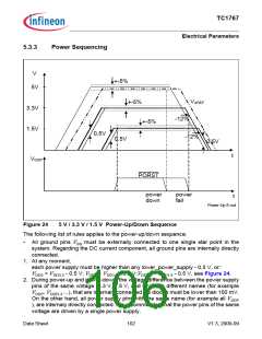
5.3.5
Phase Locked Loop (PLL)
Note: All PLL characteristics defined on this and the next page are not subject to
production test, but verified by design characterization.
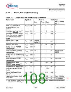
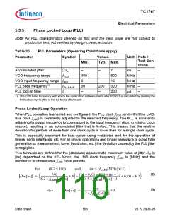
Table 20
PLL Parameters (Operating Conditions apply)
Parameter
Symbol
Values
Unit Note /
Test Con
Min.
Typ. Max.
dition
Accumulated jitter
|Dm|
–
–
7
ns
–
VCO frequency range
fVCO
400
8
–
800
16
MHz –
MHz –
MHz –
VCO input frequency range fREF
PLL base frequency1)
–
fPLLBASE
tL
50
–
200
–
320
200
PLL lock-in time
µs
–
1) The CPU base frequency with which the application software starts after PORST is calculated by dividing the
limit values by 16 (this is the K2 factor after reset).
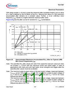
Phase Locked Loop Operation
When PLL operation is enabled and configured, the PLL clock fVCO (and with it the LMB-
Bus clock fLMB) is constantly adjusted to the selected frequency. The PLL is constantly
adjusting its output frequency to correspond to the input frequency (from crystal or clock
source), resulting in an accumulated jitter that is limited. This means that the relative
deviation for periods of more than one clock cycle is lower than for a single clock cycle.
This is especially important for bus cycles using waitstates and for the operation of
timers, serial interfaces, etc. For all slower operations and longer periods (e.g. pulse train
generation or measurement, lower baudrates, etc.) the deviation caused by the PLL jitter
is negligible.
Two formulas are defined for the (absolute) approximate maximum value of jitter Dm in
[ns] dependent on the K2 - factor, the LMB clock frequency fLMB in [MHz], and the
number m of consecutive fLMB clock periods.
for
(K2 ≤ 100)
and
(m ≤ (fLMB[MHz]) ⁄ 2)
(1 – 0, 01 × K2) × (m – 1)
0, 5 × fLMB[MHz] – 1
(2)
(3)
740
Dm[ns] = -------------------------------------------- + 5 × ---------------------------------------------------------------- + 0 , 0 1 × K2
K2 × fLMB[MHz]
740
else
Dm[ns] = -------------------------------------------- + 5
K2 × fLMB[MHz]
Data Sheet
106
V1.3, 2009-09

 INFINEON [ Infineon ]