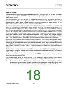
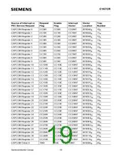
C167CR
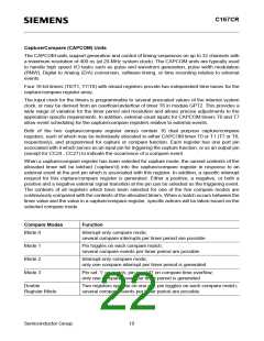
Capture/Compare (CAPCOM) Units
The CAPCOM units support generation and control of timing sequences on up to 32 channels with
a maximum resolution of 400 ns (at 20-MHz system clock). The CAPCOM units are typically used
to handle high speed I/O tasks such as pulse and waveform generation, pulse width modulation
(PMW), Digital to Analog (D/A) conversion, software timing, or time recording relative to external
events.
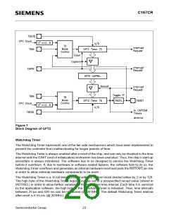
Four 16-bit timers (T0/T1, T7/T8) with reload registers provide two independent time bases for the
capture/compare register array.
The input clock for the timers is programmable to several prescaled values of the internal system
clock, or may be derived from an overflow/underflow of timer T6 in module GPT2. This provides a
wide range of variation for the timer period and resolution and allows precise adjustments to the
application specific requirements. In addition, external count inputs for CAPCOM timers T0 and T7
allow event scheduling for the capture/compare registers relative to external events.
Both of the two capture/compare register arrays contain 16 dual purpose capture/compare
registers, each of which may be individually allocated to either CAPCOM timer T0 or T1 (T7 or T8,
respectively), and programmed for capture or compare function. Each register has one port pin
associated with it which serves as an input pin for triggering the capture function, or as an output pin
(except for CC24...CC27) to indicate the occurrence of a compare event.
When a capture/compare register has been selected for capture mode, the current contents of the
allocated timer will be latched (‘capture’d) into the capture/compare register in response to an
external event at the port pin which is associated with this register. In addition, a specific interrupt
request for this capture/compare register is generated. Either a positive, a negative, or both a
positive and a negative external signal transition at the pin can be selected as the triggering event.
The contents of all registers which have been selected for one of the five compare modes are
continuously compared with the contents of the allocated timers. When a match occurs between the
timer value and the value in a capture/compare register, specific actions will be taken based on the
selected compare mode.
Compare Modes
Function
Mode 0
Interrupt-only compare mode;
several compare interrupts per timer period are possible
Mode 1
Mode 2
Mode 3
Pin toggles on each compare match;
several compare events per timer period are possible
Interrupt-only compare mode;
only one compare interrupt per timer period is generated
Pin set ‘1’ on match; pin reset ‘0’ on compare time overflow;
only one compare event per timer period is generated
Double
Register Mode
Two registers operate on one pin; pin toggles on each compare match;
several compare events per timer period are possible.
Semiconductor Group
19

 INFINEON [ Infineon ]