PDF
最近搜索
热门搜索
发布采购

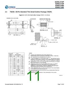
| 型号: | S29GL128P90TFIR10 |
| PDF下载: | 下载PDF文件 查看货源 |
| 内容描述: | [High Performance Page Mode] |
| 分类和应用: | PC光电二极管内存集成电路闪存 |
| 文件页数/大小: | 82 页 / 904 K |
| 品牌: |  INFINEON [ Infineon ] INFINEON [ Infineon ] |
专业IC领域供求交易平台:提供全面的IC Datasheet资料和资讯,Datasheet 1000万数据,IC品牌1000多家。