S29GL01GP
S29GL512P
S29GL256P
S29GL128P
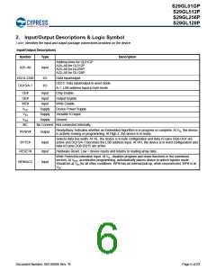
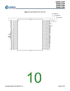
2. Input/Output Descriptions & Logic Symbol
Table identifies the input and output package connections provided on the device.
Input/Output Descriptions
Symbol
Type
Description
Address lines for GL01GP
A24–A0 for GL512P
A23–A0 for GL256P,
A22–A0 for GL128P.
A25–A0
Input
DQ14–DQ0
DQ15/A-1
I/O
I/O
Data input/output.
DQ15: Data input/output in word mode.
A-1: LSB address input in byte mode.
CE#
OE#
WE#
VCC
VIO
Input
Input
Chip Enable.
Output Enable.
Write Enable.
Input
Supply
Supply
Supply
Device Power Supply.
Versatile IO Input.
Ground.
VSS
NC
No Connect Not connected internally.
Ready/Busy. Indicates whether an Embedded Algorithm is in progress or complete. At VIL, the device
is actively erasing or programming. At High Z, the device is in ready.
RY/BY#
Output
Selects data bus width. At VIL, the device is in byte configuration and data I/O pins DQ0-DQ7 are
active and DQ15/A-1 becomes the LSB address input. At VIH, the device is in word configuration and
data I/O pins DQ0-DQ15 are active.
BYTE#
Input
Input
RESET#
Hardware Reset. Low = device resets and returns to reading array data.
Write Protect/Acceleration Input. At VIL, disables program and erase functions in the outermost
sectors. At VHH, accelerates programming; automatically places device in unlock bypass mode.
Should be at VIH for all other conditions. WP# has an internal pull-up; when unconnected, WP# is at
VIH.
WP#/ACC
Input
Document Number: 002-00886 Rev. *B
Page 6 of 83

 INFINEON [ Infineon ]