S29GL01GP
S29GL512P
S29GL256P
S29GL128P
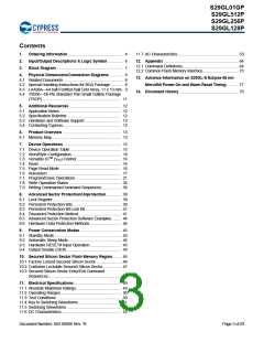
Contents
1.
2.
3.
4.
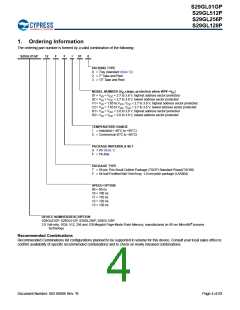
Ordering Information................................................... 4
11.7 AC Characteristics........................................................ 53
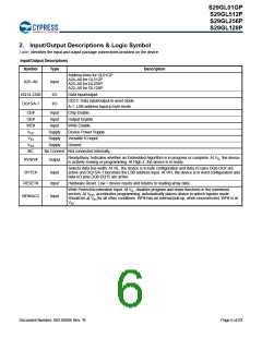
Input/Output Descriptions & Logic Symbol .............. 6
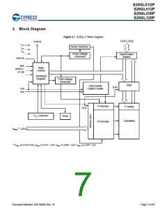
Block Diagram.............................................................. 7
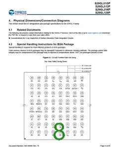
Physical Dimensions/Connection Diagrams............. 8
12. Appendix ..................................................................... 64
12.1 Command Definitions.................................................... 64
12.2 Common Flash Memory Interface................................. 73
13. Advance Information on S29GL-S Eclipse 65 nm
MirrorBit Power-On and Warm Reset Timing........... 77
14. Document History....................................................... 79
4.1 Related Documents ....................................................... 8
4.2 Special Handling Instructions for BGA Package............ 8
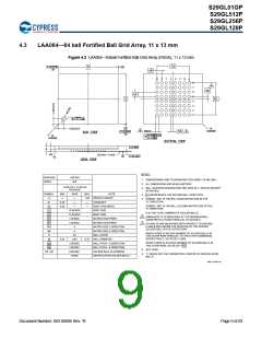
4.3 LAA064—64 ball Fortified Ball Grid Array, 11 x 13 mm. 9
4.4 TS056—56-Pin Standard Thin Small Outline Package
(TSOP)......................................................................... 11
5.
Additional Resources................................................ 12
5.1 Application Notes......................................................... 12
5.2 Specification Bulletins.................................................. 12
5.3 Hardware and Software Support.................................. 12
5.4 Contacting Cypress...................................................... 12
6.
6.1 Memory Map................................................................ 13
7. Device Operations ..................................................... 15
Product Overview ...................................................... 13
7.1 Device Operation Table ............................................... 15
7.2 Word/Byte Configuration.............................................. 16
7.3 Versatile IOTM (VIO) Control......................................... 16
7.4 Read ............................................................................ 16
7.5 Page Read Mode......................................................... 16
7.6 Autoselect .................................................................... 17
7.7 Program/Erase Operations .......................................... 21
7.8 Write Operation Status................................................. 32
7.9 Writing Commands/Command Sequences.................. 36
8.
Advanced Sector Protection/Unprotection ............. 38
8.1 Lock Register............................................................... 39
8.2 Persistent Protection Bits............................................. 39
8.3 Persistent Protection Bit Lock Bit................................. 41
8.4 Password Protection Method....................................... 41
8.5 Advanced Sector Protection Software Examples ........ 44
8.6 Hardware Data Protection Methods............................. 44
9.
Power Conservation Modes...................................... 45
9.1 Standby Mode.............................................................. 45
9.2 Automatic Sleep Mode................................................. 45
9.3 Hardware RESET# Input Operation............................. 45
9.4 Output Disable (OE#)................................................... 45
10. Secured Silicon Sector Flash Memory Region ....... 46
10.1 Factory Locked Secured Silicon Sector....................... 46
10.2 Customer Lockable Secured Silicon Sector................. 47
10.3 Secured Silicon Sector Entry/Exit Command
Sequences................................................................... 47
11. Electrical Specifications............................................ 49
11.1 Absolute Maximum Ratings ......................................... 49
11.2 Operating Ranges........................................................ 50
11.3 Test Conditions............................................................ 50
11.4 Key to Switching Waveforms ....................................... 51
11.5 Switching Waveforms .................................................. 51
11.6 DC Characteristics....................................................... 52
Document Number: 002-00886 Rev. *B
Page 3 of 83

 INFINEON [ Infineon ]