S29GL01GP
S29GL512P
S29GL256P
S29GL128P
7.2
Word/Byte Configuration
The BYTE# pin controls whether the device data I/O pins operate in the byte or word configuration. If the BYTE# pin is set at logic
‘1’, the device is in word configuration, DQ0-DQ15 are active and controlled by CE# and OE#.
If the BYTE# pin is set at logic ‘0’, the device is in byte configuration, and only data I/O pins DQ0-DQ7 are active and controlled by
CE# and OE#. The data I/O pins DQ8-DQ14 are tri-stated, and the DQ15 pin is used as an input for the LSB (A-1) address function.
7.3
Versatile IOTM (V ) Control
IO
The VersatileIOTM (VIO) control allows the host system to set the voltage levels that the device generates and tolerates on all inputs
and outputs (address, control, and DQ signals). VIO range is 1.65 to VCC. See Ordering Information on page 4 for VIO options on this
device.
For example, a VIO of 1.65-3.6 volts allows for I/O at the 1.8 or 3 volt levels, driving and receiving signals to and from other 1.8 or 3
V devices on the same data bus.
7.4
Read
All memories require access time to output array data. In a read operation, data is read from one memory location at a time.
Addresses are presented to the device in random order, and the propagation delay through the device causes the data on its outputs
to arrive with the address on its inputs.
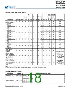
The device defaults to reading array data after device power-up or hardware reset. To read data from the memory array, the system
must first assert a valid address on Amax-A0, while driving OE# and CE# to VIL. WE# must remain at VIH. All addresses are latched
on the falling edge of CE#. Data will appear on DQ15-DQ0 after address access time (tACC), which is equal to the delay from stable
addresses to valid output data. The OE# signal must be driven to VIL. Data is output on DQ15-DQ0 pins after the access time (tOE
)
has elapsed from the falling edge of OE#, assuming the tACC access time has been meet.
7.5
Page Read Mode
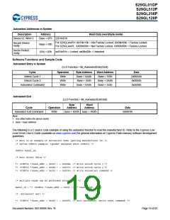
The device is capable of fast page mode read and is compatible with the page mode Mask ROM read operation. This mode provides
faster read access speed for random locations within a page. The page size of the device is 8 words/16 bytes. The appropriate page
is selected by the higher address bits A(max)-A3. Address bits A2-A0 in word mode (A2 to A-1 in byte mode) determine the specific
word within a page. The microprocessor supplies the specific word location.
The random or initial page access is equal to tACC or tCE and subsequent page read accesses (as long as the locations specified by
the microprocessor falls within that page) is equivalent to tPACC. When CE# is de-asserted and reasserted for a subsequent access,
the access time is tACC or tCE. Fast page mode accesses are obtained by keeping the “read-page addresses” constant and changing
the “intra-read page” addresses.
Document Number: 002-00886 Rev. *B
Page 16 of 83

 INFINEON [ Infineon ]