S29GL01GP
S29GL512P
S29GL256P
S29GL128P
7. Device Operations
This section describes the read, program, erase, handshaking, and reset features of the Flash devices.
Operations are initiated by writing specific commands or a sequence with specific address and data patterns into the command
registers (see Table through Table ). The command register itself does not occupy any addressable memory location; rather, it is
composed of latches that store the commands, along with the address and data information needed to execute the command. The
contents of the register serve as input to the internal state machine and the state machine outputs dictate the function of the device.
Writing incorrect address and data values or writing them in an improper sequence may place the device in an unknown state, in
which case the system must pull the RESET# pin low or power cycle the device to return the device to the reading array data mode.
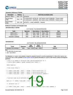
7.1
Device Operation Table
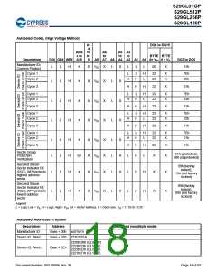
The device must be setup appropriately for each operation. Table describes the required state of each control pin for any particular
operation.
Device Operations
DQ8–DQ15
Addresses
Operation
CE#
OE# WE#
RESET# WP#/ACC
(Note 1)
DQ0–DQ7 BYTE#= VIH BYTE#= VIL
Read
L
L
H
H
X
H
H
H
H
X
(Note 2)
VHH
AIN
DOUT
(Note 3)
(Note 3)
High-Z
DOUT
(Note 3)
(Note 3)
High-Z
DQ8–DQ14
= High-Z,
DQ15 = A-1
Write (Program/
Erase)
L
L
AIN
AIN
X
Accelerated Program
L
L
VCC ± 0.3
V
VCC ± 0.3
V
Standby
X
H
High-Z
Output Disable
Reset
L
H
X
H
X
H
L
X
X
X
X
High-Z
High-Z
High-Z
High-Z
High-Z
High-Z
X
Legend
L = Logic Low = VIL, H = Logic High = VIH, VHH = 11.5–12.5V, X = Don’t Care, AIN = Address In, DIN = Data In, DOUT = Data Out
Notes
1. Addresses are AMax:A0 in word mode; AMax:A-1 in byte mode.
2. If WP# = VIL, on the outermost sector remains protected. If WP# = VIH, the outermost sector is unprotected. WP# has an internal pull-up; when
unconnected, WP# is at VIH. All sectors are unprotected when shipped from the factory (The Secured Silicon Sector can be factory protected
depending on version ordered.)
3. DIN or DOUT as required by command sequence, data polling, or sector protect algorithm.
Document Number: 002-00886 Rev. *B
Page 15 of 83

 INFINEON [ Infineon ]