®
PROFET ITS 5215L
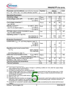
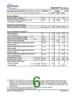
Parameter and Conditions, each of the four channels Symbol
Values
Unit
at Tj = -40...+150°C, V = 12 V unless otherwise specified
bb
min
typ
max
Reverse Battery
Reverse battery voltage 16)
-Vbb
-VON
--
--
--
600
32
-- mV
V
Drain-source diode voltage (V > V
)
out
bb
IL =-2.0A, Tj =+150°C
Diagnostic Characteristics
Open load detection voltage
V OUT(OL)
1.7
2.5
2.8
4.0
4.0
V
1
Input and Status Feedback17)
Input resistance
RI
6.0
kΩ
(see circuit page 8)
Input turn-on threshold voltage
Input turn-off threshold voltage
Input threshold hysteresis
VIN(T+)
VIN(T-)
∆ VIN(T)
td(STon)
--
1.0
--
--
--
0.2
10
2.5
--
--
V
V
V
Status change after positive input slope18)
with open load
--
20
µs
Status change after positive input slope18)
with overload
td(STon)
td(SToff)
td(SToff)
30
--
--
--
--
--
500
20
µs
µs
µs
Status change after negative input slope
with open load
Status change after negative input slope18)
with overtemperature
--
Off state input current
On state input current
Status output (open drain)
Zener limit voltage
VIN = 0.4 V: IIN(off)
VIN = 5 V: IIN(on)
5
10
--
35
20
60
µA
µA
IST = +1.6 mA: VST(high)
IST = +1.6 mA: VST(low)
5.4
--
--
--
--
0.6
V
ST low voltage
16)
Requires a 150 Ω resistor in GND connection. The reverse load current through the intrinsic drain-source
diode has to be limited by the connected load. Power dissipation is higher compared to normal operating
conditions due to the voltage drop across the drain-source diode. The temperature protection is not active
during reverse current operation! Input and Status currents have to be limited (see max. ratings page 3 and
circuit page 8).
17)
18)
If ground resistors R
are used, add the voltage drop across these resistors.
GND
not subject to production test, specified by design
Infineon Technologies AG
6
2006-Mar-27

 INFINEON [ Infineon ]