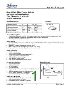
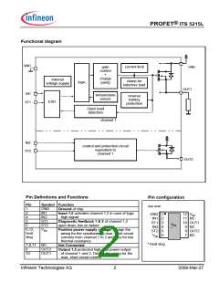
®
PROFET ITS 5215L
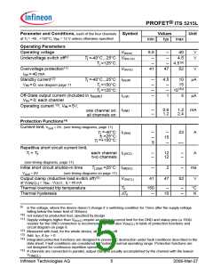
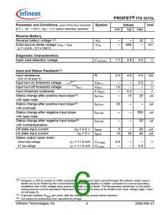
Maximum Ratings at Tj = 25°C unless otherwise specified
Parameter
Symbol
Values
Unit
Supply voltage (overvoltage protection see page 5)
Supply voltage for full short circuit protection
Vbb
Vbb
43
36
V
V
Tj,start =-40 ...+150°C
Load current (Short-circuit current, see page 6)
IL
self-limited
60
A
V
3)
Load dump protection1) VLoadDump = VA + Vs, VA = 13.5 V VLoaddump
RI2) = 2 Ω, td = 400 ms; IN= low or high,
each channel loaded with RL = 13.5 Ω,
Junction temperature
Tj
Ta
Tstg
+150
-30 ...+85
-40 … +105
°C
W
Operating temperature range
Storage temperature range
Power dissipation (DC)4)
Ta = 25°C: Ptot
Ta = 85°C:
3.1
1.6
(all channels active)
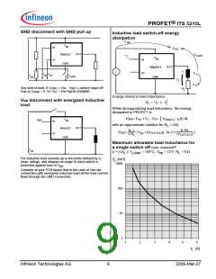
Maximal switchable inductance, single pulse
Vbb =12V, Tj,start =150°C4), see diagrams on page 9
21.3
10
1.0
4.0
8.0
mH
kV
I = 3.5 A, EAS = 178 mJ, 0Ω
IL = 7.0 A, EAS = 337 mJ, 0Ω
one channel: ZL
two parallel channels:
ElLectrostatic discharge capability (ESD)
(Human Body Model)
IN:
VESD
ST:
out to all other pins shorted:
acc. MIL-STD883D, method 3015.7 and ESD assn. std. S5.1-1993
R=1.5kΩ; C=100pF
Input voltage (DC) see internal circuit diagram page 8
Current through input pin (DC)
VIN
IIN
IINp
IST
-10 ... +16
±0.3
V
mA
Pulsed current through input pin5)
Current through status pin (DC)
±5.0
±5.0
1)
Supply voltages higher than Vbb(AZ) require an external current limit for the GND and status pins (a 150Ω
resistor for the GND connection is recommended.
2)
3)
4)
R = internal resistance of the load dump test pulse generator
I
VLoad dump is setup without the DUT connected to the generator per ISO 7637-1 and DIN 40839
Device on 50mm*50mm*1.5mm epoxy PCB FR4 with 6cm2 (one layer, 70µm thick) copper area for V
connection. PCB is vertical without blown air. See page 13
bb
5)
only for testing
Infineon Technologies AG
3
2006-Mar-27

 INFINEON [ Infineon ]