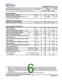
®
PROFET ITS 5215L
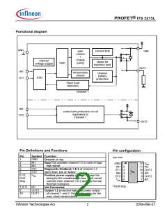
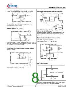
Functional diagram
GND
current limit
gate
control
+
VBB
charge
pump
internal
clamp for
logic
inductive load
OUT1
IN1
temperature
sensor
reverse
battery
ESD
ST1
protection
Open load
detection
channel 1
IN2
control and protection circuit
equivalent to
ST2
channel 1
OUT2
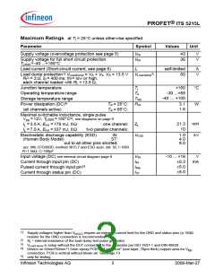
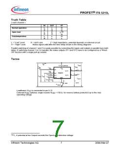
Pin Definitions and Functions
Pin configuration
Pin
1
Symbol Function
(top view)
GND
IN1
Ground of chip
2
Input 1,2 activates channel 1,2 in case of logic
high signal
GND 1•
12 V
bb
4
IN2
IN1
ST1
IN2
2
3
4
5
6
11 NC
10 OUT1
9 NC
8 OUT2
7 NC
3
ST1
ST2
Diagnostic feedback 1 & 2 of channel 1,2
open drain, low on failure
Vbb
*
5
6,12,
heat
slug
V
Positive power supply voltage. Design the
wiring for the simultaneous max. short circuit
currents from channel 1 to 2 and also for low
thermal resistance
bb
ST2
V
bb
* heat slug
7,9,11 NC
8
10
Not Connected
OUT2
OUT1
Output 1,2 protected high-side power output
of channel 1 and 2. Design the wiring for the
max. short circuit current
Infineon Technologies AG
2
2006-Mar-27

 INFINEON [ Infineon ]