CoolSET™-F3
Functional Description
3.4.3
Gate Driver
3.4
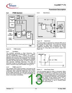
PWM Section
0.72
PWM Section
Oscillator
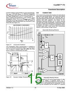
Duty Cycle
max
VCC
PWM-Latch
Clock
1
Gate
Soft Start
FF1
Comparator
CoolMOS™
Gate Driver
&
S
R
1
PWM
Comparator
Q
G8
G9
Gate Driver
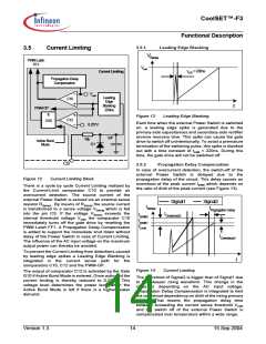
Current
Limiting
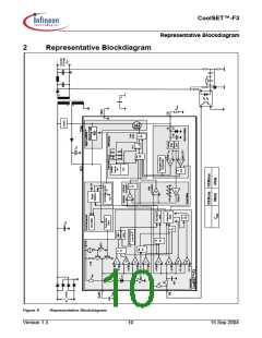
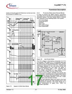
Figure 10
Gate Driver
The driver-stage is optimized to minimize EMI and to
provide high circuit efficiency. This is done by reducing
the switch on slope when exceeding the internal
CoolMOS™ threshold. This is achieved by a slope
control of the rising edge at the driver’s output (see
Figure 10).
Gate
Figure 9
3.4.1
PWM Section
Oscillator
The oscillator generates
switching frequency of ICE3Axx65x is fOSC = 100kHz
and for ICE3Bxx65x fOSC 67kHz. resistor, a
a fixed frequency. The
(internal) VGate
=
A
capacitor and a current source and current sink which
determine the frequency are integrated. The charging
and discharging current of the implemented oscillator
capacitor are internally trimmed, in order to achieve a
very accurate switching frequency. The ratio of
controlled charge to discharge current is adjusted to
reach a maximum duty cycle limitation of Dmax=0.72.
ca. t = 130ns
5V
t
3.4.2
PWM-Latch FF1
The oscillator clock output provides a set pulse to the
PWM-Latch when initiating the external Power Switch
conduction. After setting the PWM-Latch can be reset
by the PWM comparator, the Soft Start comparator or
the Current-Limit comparator. In case of resetting, the
driver is shut down immediately.
Figure 11
Gate Rising Slope
Thus the leading switch on spike is minimized. When
the integrated CoolMOS™ is switched off, the falling
shape of the driver is slowed down when reaching 2V
to prevent an overshoot below ground. Furthermore the
driver circuit is designed to eliminate cross conduction
of the output stage. During powerup when VCC is
below the undervoltage lockout threshold VVCCoff, the
output of the Gate Driver is low to disable power
transfer to the seconding side.
Version 1.3
13
15 Sep 2004

 INFINEON [ Infineon ]