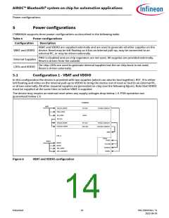
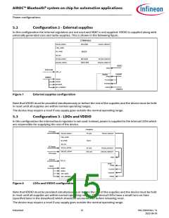
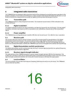
AIROC™ Bluetooth® system on chip for automotive applications
Peripherals
Most peripheral functions can be assigned to any GPIO. For details, see Table 6 and Table 7.
7.6
ADC
The CYW89820 includes a Σ-Δ ADC designed for audio and DC measurements. The ADC can measure the voltage
on 14 GPIO (P1, P9-14, P17-19, P28, P29, P32, P37). When used for analog inputs, the GPIOs must be placed in
digital input disable mode to disconnect the digital circuit from the pin and avoid leakage. The internal bandgap
reference has ±5% accuracy without calibration. Calibration and digital correction schemes can be applied to
reduce ADC absolute error and improve measurement accuracy in Direct Current (DC) Mode.
The application can access the ADC through the ADC driver included in the firmware.
7.7
PWM
The CYW89820 has four internal PWMs, labeled PWM0-3.
• Each of the six PWM channels contains the following registers:
- 16-bit initial value register (read/write)
- 16-bit toggle register (read/write)
- 16-bit PWM counter value register (read)
• PWM configuration register is shared among PWM0–3 (read/write). This 18-bit register is used:
- To enable/disable each PWM channel
- To select the clock of each PWM channel
- To invert the output of each PWM channel. The application can access the PWM module through the FW driver.
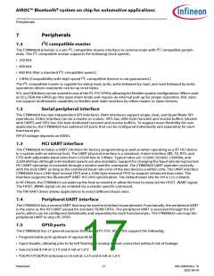
Figure 9 shows the structure of one PWM channel.
pwm_cfg_adr register
pwm#_init_val_adr register
pwm#_togg_val_adr register
16
16
pwm#_cntr_adr
16
cntr value is ARM readable
pwm_out
Example: PWM cntr w/ pwm#_init_val = 0 (dashed line)
PWM cntr w/ pwm#_init_val = x (solid line)
16'HFFFF
pwm_togg_val_adr
16'Hx
16'H000
pwm_out
Figure 9
PWM block diagram
Datasheet
18
002-25826 Rev. *G
2022-09-24

 INFINEON [ Infineon ]