AIROC™ Bluetooth® system on chip for automotive applications
Peripherals
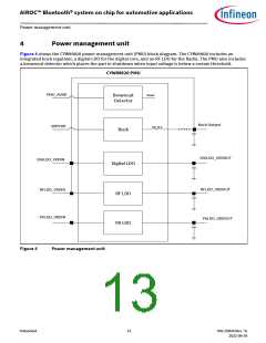
7
Peripherals
7.1
I2C compatible master
The CYW89820 provides a 2-pin I2C compatible master interface to communicate with I2C compatible periph-
erals. The I2C compatible master supports the following clock speeds:
• 100 kHz
• 400 kHz
• 800 kHz (Not a standard I2C-compatible speed.)
• 1 MHz (Compatibility with high-speed I2C-compatible devices is not guaranteed.)
The I2C compatible master is capable for doing read, write, write followed by read, and read followed by write
operations where read/write can be up to 64 bytes.
SCL and SDA lines can be routed to any of the P1-P37 GPIOs allowing for flexible system configuration. When used
as SCL/SDA the GPIOs go into open drain mode and require an external pull-up for proper operation. BSC does
not support multimaster capability or flexible wait-state insertion by either master or slave devices.
7.2
Serial peripheral interface
The CYW89820 has two independent SPI interfaces. Both interfaces support single, dual, and Quad Mode SPI
operations. Either interface can be a master or a slave. SPI1 has 1040-byte transmit and receive buffers (shared
with UART) and SPI2 has 256-byte dedicated transmit and receive buffers. To support more flexibility for user
applications, the CYW89820 has optional I/O ports that can be configured individually and separately for each
functional pin.
SPI IO voltage depends on VDDO.
7.3
HCI UART interface
The CYW89820 includes a UART interface for factory programming as well as when operating as a BT HCI device
in a system with an external host. The UART physical interface is a standard, 4-wire interface (RX, TX, RTS, and
CTS) with adjustable baud rates from 115200 bps to 3 Mbps. Typical rates are 115200, 921600, 1500000, and
3,000,000 bps although intermediate speeds are also available. Support for changing the baud rate during normal
HCI UART operation is included through a vendor-specific command. The CYW89820 UART operates correctly
with the host UART as long as the combined baud rate error of the two devices is within ±5%. The UART interface
CYW89820 has a 1040-byte receive FIFO and a 1040-byte transmit FIFO to support enhanced data rates. The
interface supports the Bluetooth® UART HCI (H4) specification. The default baud rate for H4 is 115.2 kbaud.
In HCI Mode, the CYW89820 can wake up the host as needed or allow the host to sleep via the HOST_WAKE signal.
The HOST_WAKE signal can be enabled via a vendor specific command.
The FW UART driver allows applications to select different baud rates.
7.4
Peripheral UART interface
The CYW89820 has a second UART that may be used to interface to peripherals. Functionally, the peripheral UART
is the same as the HCI UART except for 256 byte TX/RX FIFOs. The peripheral UART is accessed through the I/O
ports, which can be configured individually and separately for each functional pin. The CYW89820 can map the
peripheral UART to any LHL GPIO.
7.5
GPIO ports
The CYW89820 has 17 general purpose IOs labeled P1-P37. All GPIOs support the following:
• Programmable pull-up/down of approx 45 k
• Input disable, allowing pins to be left floating or analog signals connected without risk of leakage
• Source/sink 8 mA at 3.3 V and 4 mA at 1.8 V
• P26/P27/P28/P29 sink/source 16 mA at 3.3 V and 8 mA at 1.8 V
Datasheet
17
002-25826 Rev. *G
2022-09-24

 INFINEON [ Infineon ]