High Current PN Half Bridge
BTN8982TA
Block Description and Characteristics
5.4
Control and Diagnostics
Input Circuit
5.4.1
The control inputs IN and INH consist of TTL/CMOS compatible schmitt triggers with hysteresis which control the
integrated gate drivers for the MOSFETs. Setting the INH pin to high enables the device. In this condition one of
the two power switches is switched on depending on the status of the IN pin. To deactivate both switches, the INH
pin has to be set to low. No external driver is needed. The BTN8982TA can be interfaced directly to a
microcontroller, as long as the maximum ratings in Chapter 4.1 are not exceeded.
5.4.2
Dead Time Generation
In bridge applications it has to be assured that the highside and lowside MOSFET are not conducting at the same
time, connecting directly the battery voltage to GND. This is assured by a circuit in the driver IC, generating a so
called dead time between switching off one MOSFET and switching on the other. The dead time generated in the
driver IC is automatically adjusted to the selected slew rate.
5.4.3
Adjustable Slew Rate
In order to optimize electromagnetic emission, the switching speed of the MOSFETs is adjustable by an external
resistor. The slew rate pin SR allows the user to optimize the balance between emission and power dissipation
within his own application by connecting an external resistor RSR to GND.
5.4.4
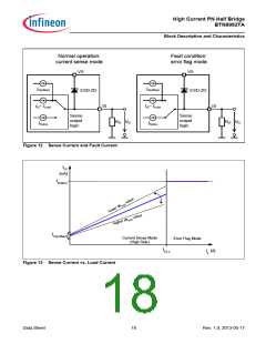
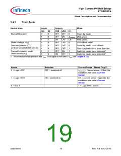
Status Flag Diagnosis with Current Sense Capability
The sense pin IS is used as a combined current sense and error flag output.
In normal operation (current sense mode), a current source is connected to the status pin, which delivers a current
proportional to the forward load current flowing through the active high side switch. The sense current can be
calculated out of the load current by the following equation:
1
---------------
IIS
=
⋅ IL + IIS(offset)
(1)
(2)
(3)
dkILIS
The other way around, the load current can be calculated out of the sense current by following equation:
IL = dkILIS ⋅ (IIS – IIS(offset)
)
The differential current sense ratio dkilis is defined by:
L2–IL1
I
--------------------------------------------
=
dkILIS
IIS(IL2)–IIS(IL1
)
If the high side drain current is zero (ISD(HS) = 0A) the offset current IIS = IIS(offset) still will be driven.
The external resistor RIS determines the voltage per IS output current. The voltage can be calculated by
.
VIS = RIS IIS.
In case of a fault condition the status output is connected to a current source which is independent of the load
current and provides IIS(lim). The maximum voltage at the IS pin is determined by the choice of the external resistor
and the supply voltage. In case of current limitation the IIS(lim) is activated for 2 * tCLS
.
Data Sheet
17
Rev. 1.0, 2013-05-17

 INFINEON [ Infineon ]