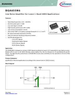
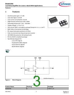
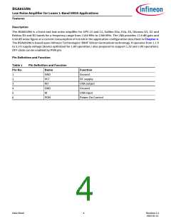
BGA855N6
Low Noise Amplifier for Lower L-Band GNSS Applications
Maximum Ratings
2
Maximum Ratings
Table 2
Maximum Ratings
Parameter
Symbol
VCC
Values
Typ.
Unit
Note or
Test Condition
Min.
-0.3
-0.3
-0.3
-0.3
-0.3
–
Max.
3.6
Voltage at pin VCC1)
Voltage at pin AI
–
–
–
–
–
–
–
–
V
–
–
–
–
–
–
–
–
VAI
0.9
V
Voltage at pin AO
Voltage at pin PON
Voltage at pin GND
Current into pin VCC
RF input power
VAO
VPON
VGND
ICC
VCC + 0.3
VCC + 0.3
0.3
V
V
V
16
mA
dBm
mW
PIN
–
+25
Total power dissipation,
Ptot
–
60
TS < 148 °C2)
Junction temperature
TJ
–
–
–
–
-
150
85
°C
°C
°C
V
–
–
–
–
Ambient temperature range
TA
-40
Storage temperature range
TSTG
-55
150
+2000
ESD capability all pins, HBM3) VESD_HBM -2000
1) All voltages refer to GND-Node unless otherwise noted
2) TS is measured on the ground lead at the soldering point
3) Human Body Model ANSI/ESDA/JEDEC JS-001 (R = 1.5kΩ, C = 100pF)
Attention: Stresses above the max. values listed here may cause permanent damage to the device.
Maximum ratings are absolute ratings; exceeding only one of these values may cause
irreversible damage to the integrated circuit. Exposure to conditions at or below absolute
maximum rating but above the specified maximum operation conditions may affect device
reliability and life time. Functionality of the device might not be given under these conditions.
Data Sheet
5
Revision 2.1
2023-01-11

 INFINEON [ Infineon ]