BGA855N6
Low Noise Amplifier for Lower L-Band GNSS Applications
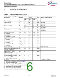
Electrical Characteristics
Table 5
TA = 25 °C, VCC = 2.8 V, VPON = 2.8 V, f = 1164 - 1300 MHz
Electrical Characteristics VCC = 2.8V1)
Parameter
Symbol
Values
Unit Note or Test Condition
Min.
1.1
–
Typ.
2.8
5.4
0.2
–
Max.
3.3
6.4
3
Supply voltage
Supply current
VCC
ICC
V
–
mA
µA
V
ON Mode
OFF Mode
ON Mode
OFF Mode
ON Mode
OFF Mode
–
–
Power on voltage
Supply current
VPON
IPON
0.8
0
VCC
0.4
10
–
V
–
5
µA
µA
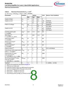
dB
–
–
1
Insertion power gain
f = 1214MHz
Noise figure2)
f = 1214 MHz, ZS = 50 Ω
Input return loss3)
f = 1214 MHz
Output return loss3)
f = 1214 MHz
Reverse isolation3)
f = 1214 MHz
Power on time4)7)
|S21|2
NF
16.9
17.9
18.9
–
0.60
13
1.10
dB
dB
dB
dB
–
–
–
–
RLIN
RLOUT
1/|S12|2
tS
10
12
19
–
–
–
20
22
–
3
5
–
µs
OFF to ON Mode
–
Inbandinput1dB-compression IP1dB
point, f = 1214 MHz3)
-12
-8
dBm
Inband input 3rd-order
IIP3
IIP3OOB
k
-4
1
2
–
–
–
–
dBm
dBm
–
intercept point3)5)
f1 = 1214 MHz, f2 = f1 +/- 1 MHz
Out of band input 3rd-order
-3
–
intercept point6)7)
f1 = 1850 MHz, f2 = 2500 MHz
Stability7)
> 1
f = 20 MHz ... 10 GHz
1) Based on the application described in Chapter 4
2) PCB losses are subtracted
3) Verification based on AQL; not 100% tested in production
4) LNA Gain changed to 90% of final gain value (in dB)
5) Input power = -30 dBm for each tone
6) Input power = -25 dBm for each tone
7) Guaranteed by device design; not tested in production
Data Sheet
8
Revision 2.1
2023-01-11

 INFINEON [ Infineon ]