SPP11N80C3
SPA11N80C3
Electrical Characteristics
Parameter
Symbol
Conditions
Values
typ. max.
Unit
S
min.
Transconductance
g
V
≥2*I *R ,
DS DS(on)max
-
7.5
-
fs
D
I =7.1A
D
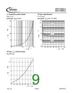
Input capacitance
C
C
C
C
V
=0V, V =25V,
GS DS
-
-
-
-
1600
800
40
-
-
-
-
pF
iss
f=1MHz
Output capacitance
oss
rss
Reverse transfer capacitance
4)
V
V
=0V,
GS
44.3
Effective output capacitance,
energy related
o(er)
=0V to 480V
DS
5)
-
33.9
-
Effective output capacitance,
time related
C
o(tr)
Turn-on delay time
t
V
=400V, V =0/10V,
GS
-
-
-
-
25
15
72
7
-
-
82
10
ns
d(on)
DD
I =11A,
Rise time
t
D
r
R =7.5Ω
Turn-off delay time
Fall time
t
G
d(off)
t
f
Gate Charge Characteristics
Gate to source charge
Gate to drain charge
Q
Q
Q
V
=640V, I =11A
-
-
-
6
25
50
-
-
60
nC
V
gs
gd
g
DD
D
V
V
=640V, I =11A,
Gate charge total
DD
D
=0 to 10V
GS
V
=640V, I =11A
-
6
-
Gate plateau voltage
V(plateau)
DD
D
1
2
Limited only by maximum temperature
Repetitve avalanche causes additional power losses that can be calculated as P =E *f.
AR
AV
3
4
Soldering temperature for TO-263: 220°C, reflow
C
is a fixed capacitance that gives the same stored energy as C
while V is rising from 0 to 80% V
.
oss
DS
o(er)
o(tr)
DSS
5
C
is a fixed capacitance that gives the same charging time as C
while V is rising from 0 to 80% V
.
oss
DS
DSS
Rev. 2.4
Page 3
2005-08-24

 INFINEON [ Infineon ]