IDT72T7285/72T7295/72T72105/72T72115 2.5V TeraSync
16,384 x 72, 32,768 x 72, 65,536 x 72, 131,072 x 72
72-BIT FIFO
COMMERCIAL AND INDUSTRIAL
TEMPERATURE RANGES
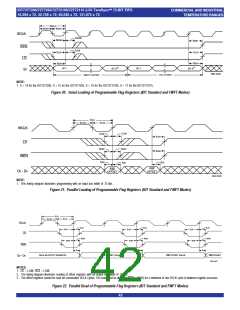
t
SCLK
tSCKH
t
SCKL
SENS
SCLK
tSENH
t
tENH
SEN
LD
tLDS
tLDS
tLDH
tSDH
t
SDS
BIT X(1)
BIT X(1)
BIT 1
BIT 1
SI
5994 drw25
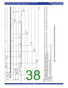
FULL OFFSET
EMPTY OFFSET
NOTE:
1. X = 14 for the IDT72T7285, X = 15 for the IDT72T7295, X = 16 for the IDT72T72105, X = 17 for the IDT72T72115.
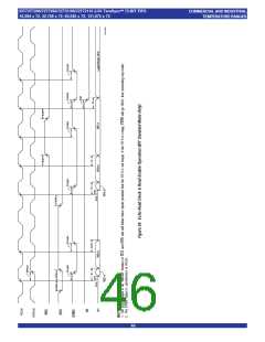
Figure 20. Serial Loading of Programmable Flag Registers (IDT Standard and FWFT Modes)
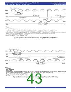
tCLK
tCLKH
tCLKL
WCLK
LD
tLDH
tLDS
tLDH
tENH
t
ENS
tENH
WEN
t
DS
tDH
t
DH
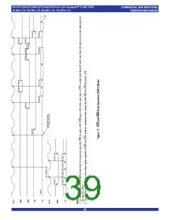
PAF
OFFSET
PAE
OFFSET
D0 - Dn
5994 drw26
NOTE:
1. This timing diagram illustrates programming with an input bus width of 72 bits.
Figure 21. Parallel Loading of Programmable Flag Registers (IDT Standard and FWFT Modes)
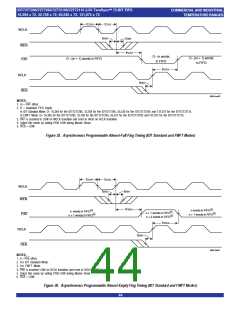
tCLK
tCLKH
tCLKL
RCLK
tLDH
tLDH
tLDH
tLDS
tLDS
tLDS
LD
tENH
tENH
tENH
t
ENS
t
ENS
tENS
REN
t
A
t
A
tA
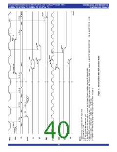
DATA IN OUTPUT REGISTER
PAE OFFSET VALUE
PAF OFFSET VALUE
PAE OFFSET
Q0 - Qn
5994 drw27
NOTES:
1. OE = LOW; RCS = LOW.
2. The timing diagram illustrates reading of offset registers with an output bus width of 72 bits.
3. The offset registers cannot be read on consecutive RCLK cycles. The read must be disabled (REN = HIGH) for a minimum of one RCLK cycle in between register accesses.
Figure 22. Parallel Read of Programmable Flag Registers (IDT Standard and FWFT Modes)
42

 IDT [ INTEGRATED DEVICE TECHNOLOGY ]