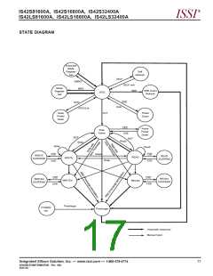
®
IS42S81600A, IS42S16800A, IS42S32400A
IS42LS81600A, IS42LS16800A, IS42LS32400A
ISSI
(1,2,3)
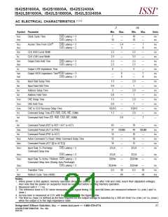
AC ELECTRICAL CHARACTERISTICS
-7
-10
Min.
Symbol Parameter
Min.
Max.
Max
Units
tCK3
tCK2
Clock Cycle Time
CAS Latency = 3
CAS Latency = 2
7
10
—
—
10
10
—
—
ns
ns
tAC3
tAC2
Access Time From CLK(4)
CAS Latency = 3
CAS Latency = 2
—
—
5.4
6
—
—
7
9
ns
ns
tCHI
tCL
CLK HIGH Level Width
CLK LOW Level Width
Output Data Hold Time
2.5
2.5
—
—
3.5
3.5
—
—
ns
ns
tOH3
tOH2
CAS Latency = 3
CAS Latency = 2
2.5
2.5
—
—
2.5
2.5
—
—
ns
ns
tLZ
Output LOW Impedance Time
0
—
0
—
ns
tHZ3
tHZ2
Output HIGH Impedance Time(5)CAS Latency = 3
CAS Latency = 2
—
—
6
6
—
—
7
9
ns
ns
tDS
Input Data Setup Time
1.5
0.8
.5
—
—
—
—
—
—
—
—
0.8
2.0
1
—
—
—
—
—
—
—
—
1
ns
ns
ns
ns
ns
ns
ns
ns
—
tDH
Input Data Hold Time
tAS
Address Setup Time
2.0
1
tAH
Address Hold Time
0.8
1.5
0.8
tCKS
tCKH
tCKA
tCS
CKE Setup Time
2.0
1
CKE Hold Time
CKE to CLK Recovery Delay Time
Command Setup Time (CS, RAS, CAS, WE, DQM)
Command Hold Time (CS, RAS, CAS, WE, DQM)
1CLK+3
1.5
1CLK+3
2.0
—
tCH
ns
tRC
Command Period (REF to REF / ACT to ACT)
Command Period (ACT to PRE)
63
37
—
120,000
—
70
44
—
120,000
—
ns
ns
ns
ns
ns
ns
tRAS
tRP
Command Period (PRE to ACT)
15
18
tRCD
tRRD
tDPL3
Active Command To Read / Write Command Delay Time
Command Period (ACT [0] to ACT[1])
15
—
18
—
14
—
15
—
Input Data To Precharge
Command Delay time
CAS Latency = 3
2CLK
—
2CLK
—
tDPL2
tDAL3
CAS Latency = 2
2CLK
—
—
2CLK
—
—
ns
ns
Input Data To Active / Refresh CAS Latency = 3
Command Delay time (During Auto-Precharge)
CAS Latency = 2
CLK+tRP
2CLK+tRP
tDAL2
tT
2CLK+tRP
0.5
—
30
64
2CLK+tRP
0.5
—
30
64
ns
ns
Transition Time
tREF
Refresh Cycle Time (4096)
—
—
ms
Notes:
1. When power is first applied, memory operation should be started 100 µs after Vdd and VddQ reach their stipulated voltages.
Also note that the power-on sequence must be executed before starting memory operation.
2. Measured with tT = 1 ns.
3. The reference level is 0.9V when measuring input signal timing. Rise and fall times are measured between VIH (min.) and VIL
(max.).
4. Access time is measured at 0.9V with the load shown in the figure below.
5. The time tHZ (max.) is defined as the time required for the output voltage to transition by ± 200 mV from VOH (min.) or VOL (max.)
when the output is in the high impedance state.
Integrated Silicon Solution, Inc. — www.issi.com — 1-800-379-4774
ADVANCEDINFORMATION Rev. 00A
21
06/01/02

 ICSI [ INTEGRATED CIRCUIT SOLUTION INC ]