®
IS42S81600A, IS42S16800A, IS42S32400A
IS42LS81600A, IS42LS16800A, IS42LS32400A
ISSI
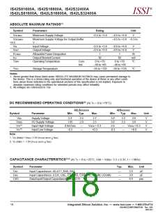
ABSOLUTE MAXIMUM RATINGS(1)
Symbol
Parameters
Rating
Unit
VDD MAX
Maximum Supply Voltage
–0.5 to +3.6
–0.5 to +4.6
V
VDDQMAX
+4.6
Maximum Supply Voltage for Output Buffer
V
–0.5 to +3.6 –0.5 to
VIN
InputVoltage
–0.5 to +3.6
–0.5 to +4.6
V
V
VOUT
PD MAX
ICS
OutputVoltage
–0.5 to +3.6
–0.5 to +4.6
AllowablePowerDissipation
OutputShortedCurrent
1
1
W
50
50
mA
°C
TOPR
OperatingTemperature
Com.
Ind.
0 to +70
–40 to +85
0 to +70
–40 to +85
TSTG
StorageTemperature
–55 to +125
–55 to +125
°C
Notes:
1. Stress greater than those listed under ABSOLUTE MAXIMUM RATINGS may cause permanent damage to
the device. This is a stress rating only and functional operation of the device at these or any other condi-
tions above those indicated in the operational sections of this specification is not implied. Exposure to
absolute maximum rating conditions for extended periods may affect reliability.
2. All voltages are referenced to Vss.
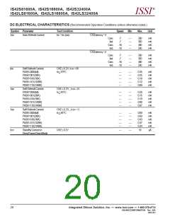
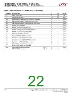
DC RECOMMENDED OPERATING CONDITIONS(2) (At TA = 0 to +70°C)
42LSxxxxxx
Typ.
42Sxxxxxx
Typ.
Symbol
Parameter
Min.
Max.
Min.
Max.
Unit
VDD
SupplyVoltage
2.3
2.5
2.0
2.7
2.5
3.0
3.0
2.0
-0.3
3.3
3.3
3.6
3.6
V
V
V
V
VDDQ
I/O Supply Voltage
Input High Voltage
Input Low Voltage
1.65
(1)
VIH
0.8xVDDQ
-0.3
—
—
VDDQ + 0.3
+0.3
—
—
VDDQ + 0.3
+0.8
(2)
VIL
Note:
1. VIH (max) = VDDQ +1.5V (PULSE WIDTH < 5NS).
2. VIL (min) = -1.5V (PULSE WIDTH < 5NS).
CAPACITANCE CHARACTERISTICS(1,2) (At TA = 0 to +25°C, Vdd = VddQ= 3.3 ± 0.3V, f = 1 MHz)
Symbol
Parameter
Typ.
Max.
Unit
CIN1
CIN2
CI/O
Input Capacitance: A0-A11, BA0, BA1
—
—
—
3.5
3.8
6.5
pF
pF
Input Capacitance: (CLK, CKE, CS, RAS, CAS, WE, LDQM, UDQM)
DataInput/OutputCapacitance:I/O0-I/O15
pss.
18
Integrated Silicon Solution, Inc. — www.issi.com — 1-800-379-4774
ADVANCEDINFORMATION Rev. 00A
06/01/02

 ICSI [ INTEGRATED CIRCUIT SOLUTION INC ]