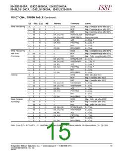
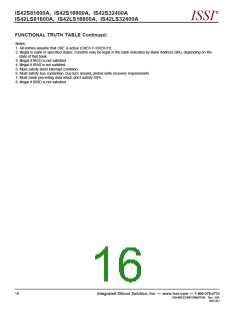
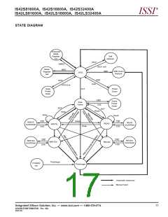
®
IS42S81600A, IS42S16800A, IS42S32400A
IS42LS81600A, IS42LS16800A, IS42LS32400A
ISSI
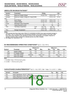
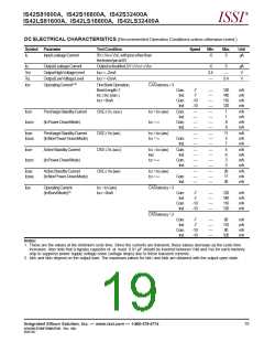
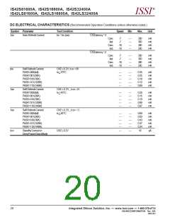
DC ELECTRICAL CHARACTERISTICS (Recommended Operation Conditions unless otherwise noted.)
Symbol Parameter
TestCondition
Speed
Min.
Max.
Unit
IIL
InputLeakageCurrent
0V≤VIN ≤VDD,withpinsotherthan
–5
5
µA
thetestedpinat0V
I
OL
OH
OL
OutputLeakageCurrent
OutputHighVoltageLevel
OutputLowVoltageLevel
OperatingCurrent(1,2)
Outputisdisabled,0V≤VOUT ≤VDD
–5
2.4
—
5
µA
V
V
IOUT =–2mA
—
0.4
V
IOUT=+2mA
V
IDD1
OneBankOperation,
BurstLength=1
CASlatency=3
Com.
Ind.
Com.
Ind.
-7
-7
-10
-10
—
—
—
—
120
140
110
120
mA
mA
mA
mA
tRC ≥tRC (min.)
IOUT=0mA
I
DD2P
PrechargeStandbyCurrent
(InPower-DownMode)
CKE≤VIL
(
MAX
)
t
CK =tCK
(MIN
)
Com.
Ind.
Com.
Ind.
—
—
—
—
—
—
—
—
1
1
.6
.6
mA
mA
mA
mA
IDD2PS
tCK =∞
I
DD2N
PrechargeStandbyCurrent
(InNonPower-DownMode)
CKE≥VIH
CKE≤VIL
(
MIN
)
t
CK =tCK
(
MIN
)
)
—
—
—
—
—
—
11
5
7
mA
mA
mA
IDD2NS
tCK =∞
Com.
Ind.
IDD3P
ActiveStandbyCurrent
(InPower-DownMode)
(MAX
)
tCK =tCK
(MIN
Com.
Ind.
Com.
Ind.
—
—
—
—
—
—
—
—
4
6
3
5
mA
mA
mA
mA
Ind.
IDD3PS
tCK =∞
I
DD3N
ActiveStandbyCurrent
(InNonPower-DownMode)
CKE≥VIH
(MIN
)
t
CK =tCK
(MIN
)
—
—
—
—
—
—
28
17
20
mA
mA
mA
IDD3NS
tCK =∞
Com.
Ind.
IDD4
OperatingCurrent
(InBurstMode)(1)
t
CK =tCK
(
MIN
)
CASlatency=3
CASlatency=2
IOUT=0mA
Com.
Ind.
Com.
Ind.
-7
-7
-10
-10
—
—
—
—
120
140
110
120
mA
mA
mA
mA
Com.
Ind.
Com.
Ind.
-7
-7
-10
-10
—
—
—
—
90
110
80
mA
mA
mA
mA
100
Notes:
1. These are the values at the minimum cycle time. Since the currents are transient, these values decrease as the cycle time
increases. Also note that a bypass capacitor of at least 0.01 µF should be inserted between Vdd and Vss for each memory
chip to suppress power supply voltage noise (voltage drops) due to these transient currents.
2. Idd1 and Idd4 depend on the output load. The maximum values for Idd1 and Idd4 are obtained with the output open state.
Integrated Silicon Solution, Inc. — www.issi.com — 1-800-379-4774
ADVANCEDINFORMATION Rev. 00A
19
06/01/02

 ICSI [ INTEGRATED CIRCUIT SOLUTION INC ]