ICS511
TM
LOCO PLL Clock Multiplier
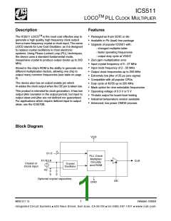
used. The device crystal connections should include
pads for small capacitors from X1 to ground and from
X2 to ground. These capacitors are used to adjust the
stray capacitance of the board to match the nominally
required crystal load capacitance. Because load
capacitance can only be increased in this trimming
process, it is important to keep stray capacitance to a
minimum by using very short PCB traces (and no vias)
between the crystal and device. Crystal capacitors, if
needed, must be connected from each of the pins X1
and X2 to ground.
External Components
Decoupling Capacitor
As with any high-performance mixed-signal IC, the
ICS511 must be isolated from system power supply
noise to perform optimally.
A decoupling capacitor of 0.01µF must be connected
between VDD and the GND. It must be connected
close to the ICS511 to minimize lead inductance. No
external power supply filtering is required for the
ICS511.
The value (in pF) of these crystal caps should equal
(C -12 pF)*2. In this equation, C = crystal load
L
L
Series Termination Resistor
A 33Ω terminating resistor can be used next to the CLK
pin for trace lengths over one inch.
capacitance in pF. Example: For a crystal with a 16 pF
load capacitance, each crystal capacitor would be 8 pF
[(16-12) x 2] = 8.
Crystal Load Capacitors
The total on-chip capacitance is approximately 12 pF. A
parallel resonant, fundamental mode crystal should be
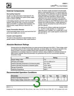
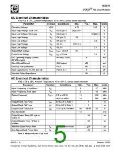
Absolute Maximum Ratings
Stresses above the ratings listed below can cause permanent damage to the ICS511. These ratings, which
are standard values for ICS commercially rated parts, are stress ratings only. Functional operation of the
device at these or any other conditions above those indicated in the operational sections of the
specifications is not implied. Exposure to absolute maximum rating conditions for extended periods can
affect product reliability. Electrical parameters are guaranteed only over the recommended operating
temperature range.
Item
Rating
Supply Voltage, VDD
All Inputs and Outputs
7 V
-0.5 V to VDD+0.5 V
0 to +70°C
Ambient Operating Temperature (Commercial grade)
Ambient Operating Temperature (Industrial grade)
Storage Temperature
-40 to +85°C
-65 to +150°C
260°C
Soldering Temperature
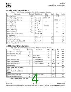
Recommended Operation Conditions
Parameter
Min.
Typ.
Max.
+85
Units
°C
Ambient Operating Temperature
Power Supply Voltage (measured in respect to GND)
-40
+3.135
+5.25
V
MDS 511 G
3
Revision 102504
Integrated Circuit Systems ● 525 Race Street, San Jose, CA 95126 ● tel (408) 297-1201 ● www.icst.com

 ICSI [ INTEGRATED CIRCUIT SOLUTION INC ]