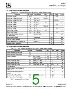
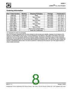
ICS511
TM
LOCO PLL Clock Multiplier
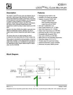
Pin Assignment
Clock Output Table
S1
0
S0
0
CLK
4X input
X1/ICLK
VDD
8
7
6
5
1
2
3
4
X2
0
M
1
5.333X input
5X input
OE
S0
0
M
M
M
1
0
2.5X input
2X input
GND
S1
M
1
CLK
3.333X input
6X input
0
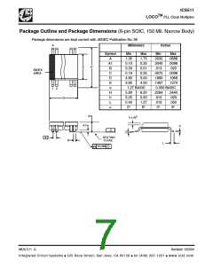
8 Pin (150 mil) SOIC
1
M
1
3X input
1
8X input
0 = connect directly to ground
1 = connect directly to VDD
M = leave unconnected (floating)
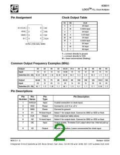
Common Output Frequency Examples (MHz)
Output
Input
20
24
12
30
10
32
16
33.33
16.66
M, M
37.5
15
40
10
48
12
50
20
60
10
64
16
10
Selection (S1, S0) M, M
M, M
1, M
M, M
M, 0
0, 0
0, 0
M, 0
1, 0
0, 0
Output
Input
66.66
72
12
75
25
80
10
83.33
25
90
15
100
20
120
15
125
25
133.3 150
20
25
25
Selection (S1, S0) M, 1
1, 0
1, M
1, 1
M, 1
1, 0
0, 1
1, 1
0, 1
0, M
1, 0
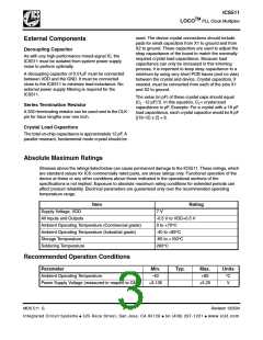
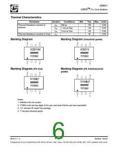
Pin Descriptions
Pin
Pin
Pin
Type
Pin Description
Number Name
1
2
3
4
5
6
7
XI/ICLK
VDD
GND
S1
Input
Power
Power
Crystal connection or clock input.
Connect to +3.3 V or +5 V.
Connect to ground.
Tri-level Iinput
Output
Select 1 for output clock. Connect to GND or VDD or float.
Clock output per table above.
CLK
S0
Tri-level Input
Input
Select 0 for output clock. Connect to GND or VDD or float.
OE
Output enable. Tri-states CLK output when low. Internal pull-up
resistor.
8
X2
Output
Crystal connection. Leave unconnected for clock input.
MDS 511 G
2
Revision 102504
Integrated Circuit Systems ● 525 Race Street, San Jose, CA 95126 ● tel (408) 297-1201 ● www.icst.com

 ICSI [ INTEGRATED CIRCUIT SOLUTION INC ]