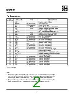
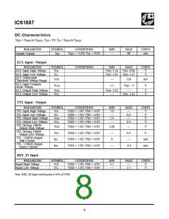
ICS1887
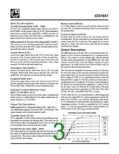
Loopback
This circuit provides the PECL to CMOS conversion for less
than $0.80 in single unit quantities. Note that the LM393 has
two amplifiers, so the unused one is tied inactive.
The AMD PDR & PDT chips have an external loopback con-
nection between the two chips. The ICS1887 also has a
loopback function, but it is totally internal to the device.
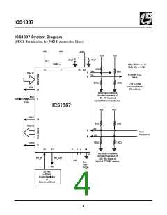
A running production change will be made to the ICS1887 to
change the CD input to PECL. Therefore, boards should be
laid out with a direct normal PECL termination connection
stuffing option. This allows either version of the part to be
used by stuffing one of two sets of external components. A
version of this circuit is shown in the diagram on the previous
page.
Optical Transmitter Off Control
The PDT chip has an input (FOTOFF) which can force an
optical transceiver to be off. The ICS1887 performs the same
behavior with the TXOFF~ pin.
Test Mode
Both the AMD PDR & PDT have a test mode that allows auto-
mated testers to test internal logic without the PLL clock
multiplier. The ICS1887 does not have a similar test mode.
With ICS1887 devices that have a TTL-compatible CD input,
the “Differential PECL to CMOS Conversion Circuit” com-
ponents need to be placed on the PCB and the “Normal PECL
Transceiver Termination” resistors (82Ω and 130Ω) as well as
the option select jumper should NOT be placed.
Transmit Current Selection
The ICS1887 allows the PECL transmit current level to be set
externally. An 887Ω resistor to the VDD supply is recom-
mended.
When the final ICS1887 device with the PECL CD input is
used, none of the components in the “Differential PECL to
CMOS Conversion Circuit” or the “Unused amp connection”
circuits should be used. Only the four termination resistors
(87Ω and 130Ω) and the option select jumper are needed.
Note that these resistors should be located near the ends of the
transmission lines.
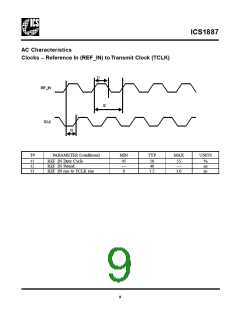
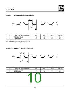
Clocking
Parallel data that is to be serialized for transmission must be
presented to the data transmitter device with a certain amount
of setup and hold time to a given clock.
The PDT chip expects data to setup relative to the 25 MHz
Local Symbol Clock (LSCLK). This clock is an input to the
device.
The ICS1887 expects data to be setup relative to the 25 MHz
Reference In Clock (REF_IN). This clock is an input to the
ICS1887 device. Note that the REF_IN pin of the ICS1887 is
a CMOS input with a switching point of 50% of VDD. If this
pin is driven by a TTL output, a pull-up resistor to VDD must
be used. The ICS1887 device also provides a Transmit Clock
(TXC) output, which is a 50% duty cycle (nominal) copy of
the REF_IN input. The ICS1887 is designed to provide a very
low skew between the REF_IN and the TCLK.
6

 ICSI [ INTEGRATED CIRCUIT SOLUTION INC ]