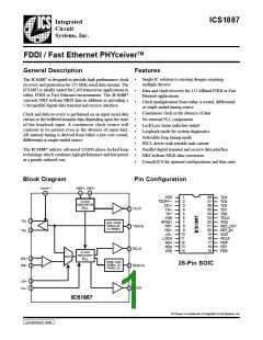
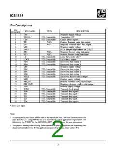
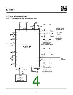
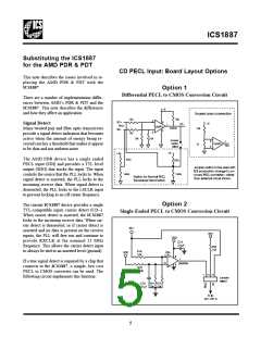
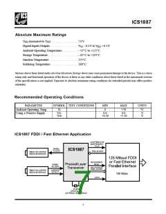
ICS1887
Input Pin Descriptions
Parallel Transmit Data (TD0 .. TD4)
Five bit TTL compatible digital input, which is received by
the ICS1887 on the positive edge of TCLK. High impedance
input drivers routed to the serial NRZ to NRZI converter. In
loopback testing mode, this NRZI data is multiplexed to the
input of the device clock recovery section.
Receive Clock (RCLK)
A 25 MHz digital clock recovered with the internal clock
recovery PLL. In loopback mode this clock is recovered from
the transmit data.
Lock/Loss Detect (LOCK)
Set high when the clock recovery PLL has locked onto the
incoming data. Set low when there is no incoming data, which
in turn causes the PLL to free-run. This signal can be used to
indicate or ‘alarm’ the next receive stage that the incoming
serial data has stopped.
Differential ECL Receive Data Input (RX+ & RX-)
The clock recovery and data regenerator from the receive
buffer are driven from this PECL input. During loopback test-
ing mode this input is ignored.
Output Description
The differential driver for the TX is current mode and is de-
Carrier Detect (CD~)
±
Active low input which forces the VCO to free run. Upon
receipt of a loss of input signal (such as from an optical-to-
electrical transducer), the internal phase-lock loop will
free-run at the selected operating frequency. Also, when
asserted, CD will set the lock output low.
signed to drive resistive terminations in a complementary
fashion. The output is current-sinking only, with the amount
of sink current programmable via the IPRG1 pin. The sink
current is equal to four times the IPRG1 current. For most
applications, an 910Ω resistor from VDD to IPRG1 will set
the current to the necessary precision.
Transmitter Off (TXOFF~)
Active low input which, when low, forces TX+ low and The TX± pins are incapable of sourcing current, so VOH must
TX-high. When high, data passes through TX+ and TX- be set by the ratios of the Thevenin termination resistors for
unaffected. This input has an internal pull-up resistor.
each of these lines. R1 is a pull-up resistor connected from the
PECL output to VDD. R2 is a pull-down resistor connected
from the PECL output to VSS. R1 and R2 are electrically in
parallel from an AC standpoint. If we pick a target impedance
of 50Ω for our transmission line impedance, a value of 62Ω
for R1 and a value of 300Ω for R2 would yield a Thevinin
equivalent characteristic impedance of 50Ω and a VOH value
of VDD -.88 volts, compatible with PECL circuits.
Loopback Mode (LB~)
Active low input which causes the clock recovery PLL to
operate using the transmit input data reference and ignore the
±
receive RX data. Utilized for system loopback testing.
External Crystal or Reference Clock
(REF_IN and REF_OUT)
This oscillator input can be driven from either a fundamental
mode crystal or a stable reference. For either method, the ref-
erence frequency is 25.00 MHz.
To set a value for VOL, we must determine a value for I that
prg
will cause the output FET’s to sink an appropriate current. We
desire VOL to beVDD -1.81 or greater. Setting up a sink current
of 19 milliamperes would guarantee this through our output
terminating resistors. As this is controlled by a 4/1 current
Output Pin Descriptions
Differential ECL Transmit Data (TX+ and TX-)
This differential output is converted TD[0..4] serial data. This
output remains active during loopback mode.
mirror, 4.75 mA into I
should set this current properly. An
prg
910Ω resistor from VDD to I
should work fine.
prg
Transmit Clock (TCLK)
TTL compatible 25 MHz clock used by the parallel processor
transmitter for clocking out transmit data. This clock can be
derived from either an independent clock source or from the
recovered data clock (system loop time mode).
Parallel Receive Data (RD0 .. RD4)
The regenerated five bit parallel data derived from the serial
data input. In loopback mode this data is regenerated from the
transmit data. This data is phase-aligned with the negative
edge of RCLK clock output.
3

 ICSI [ INTEGRATED CIRCUIT SOLUTION INC ]