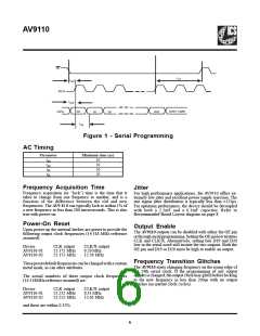
AV9110
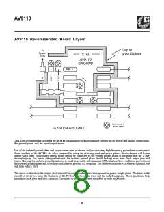
AV9110 Recommended Board Layout
This is the recommended layout for the AV9110 to maximize clock performance. Shown are the power and ground connections,
the ground plane, and the input/output traces.
Use of the isolated ground plane and power connection, as shown, will prevent stray high frequency ground and system noise
from coupling to the AV9110. As when compared to using the system ground and power planes, this technique will lessen
output clock jitter. The isolated ground plane should be connected to the system ground plane at one point near the 2.2mF
decoupling cap. For lowest jitter performance, the isolated ground plane should be kept away from clock output pins and
traces. Keeping the isolated ground plane area as small as possible will minimize EMI radiation. Use a sufficient gap between
the isolated ground plane and system ground plane to prevent AC coupling. The ferrite bead in the VDD line is optional, but
will help reduce EMI.
The traces to distribute the output clocks should be over an unbroken system ground or power supply plane. The trace width
should be about two times the thickness of the PC board between the trace and the underlying plane. These guidelines help
minimize clock jitter and EMI radiation. The traces to distribute power should be as wide as possible.
8

 ICSI [ INTEGRATED CIRCUIT SOLUTION INC ]