iC-MR 13-BIT S&H SIN/COS
INTERPOLATOR WITH CONTROLLER INTERFACES
Rev A1, Page 6/44
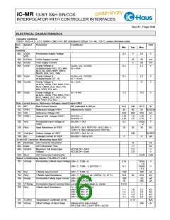
ELECTRICAL CHARACTERISTICS
Operating conditions:
VDDA = VDD = 4.5...5.5 V, GNDA = GND = 0 V, IBP calibrated to 200 µA, Tj = -40...125 °C, unless otherwise noted.
Item Symbol
No.
Parameter
Conditions
Unit
Min.
Typ.
Max.
General
001 VDDA,
VDD
Permissible Supply Voltage
4.5
5
5.5
V
002 I(VDDA)
003 I(VDD)
VDDA Supply Current
VDD Supply Current
Clamp Voltage hi
at digital inputs ASLI, SLI, MAI, I() = 4 mA
NCS, NL, NRD, NWR, NRES,
NERR, SDA, SCL, TMS
25
5
50
50
mA
mA
V
004
Vc()hi
Vc()hi = V() - V(VDD),
0.3
0.3
1.2
005
Vc()hi
Clamp Voltage hi
at digital inputs D(7...0)
Vc()hi = V() - V(VDD),
I() = 1.6 mA
1.2
11
V
V
006 Vcz()hi
007 Vc()lo
Clamp Voltage hi
I() = 4 mA
at ACO, VDDA, PSO, NSO, PCO,
NCO, AMAO, SLO, ADC, PSI,
NSI, VREF, PCI, NCI
Clamp Voltage lo
I() = -4 mA
-1.2
-0.3
V
at ACO, VDDA, PSO, NSO, PCO,
NCO, AMAO, SLO, ADC, PSI,
NSI, VREF, PCI, NCI
Bias Current Source, Reference Voltages, Input/Output VREF
101 IBP
102 VPAH
103 V05
Bias Current Source
IBP calibrated to 200 µA
referenced to GNDA
92.5
45
100
50
107.5
55
%
Reference Voltage VPAH
Reference Voltage V05
Internal Ref. Voltage VREFI
%VDDA
mV
450
500
550
104
VREFI
DCPOS = 1
DCPOS = 0
1.35
2.25
1.5
2.5
1.65
2.75
V
V
105 Vin()
106 Rin()
Permissible Input Voltage at
VREF
SELREF = 0x3
0.5
VDDA
− 2
30
V
Input Resistance at VREF
SELREF = 0x3, REFVOS = 0x3, UIN = 1,
TUIN = 0, Rin() referenced to VREFin()
20
26
kΩ
107 Vref()out
108 I0()
Output Voltage at VREF
Leakage Current at VREF
SELREF = 0x2, I() = 0
SELREF = 0x0 or 0x1
100
%VREFI
µA
-1
+1
12-bit A/D Converter, Measuring Input ADC
601 RESOadc A/D Converter Resolution
12
bit
602 t()adc
603
A/D Conversion Time
1.1
ms
Vin()FS
Maximum Full Scale Input
Voltage
ADCSLOP = 0xFF
ADCSLOP = 0x00
2.5
2.0
V
V
604 INL()
A/D Conversion Nonlinearity
±0.95
LSB
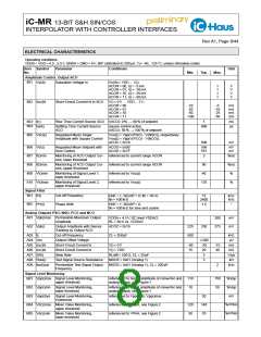
Signal Conditioning, Inputs: PSI, NSI, PCI, NCI
701
Vin()sig
Permissible V Mode Input Voltage
UIN = 1, TUIN = 0
0.75
-0.1
VDDA
− 1.5
VDDA
+ 0.1
V
V
UIN = 1, TUIN = 1, DCPOS = 1
702 Iin()
703 Rin()
V Mode Input Current
UIN = 1, TUIN = 0
-100
16.4
100
nA
V Mode Input Resistance
Permissible I Mode Input Current
UIN = 1, TUIN = 1, vs. VREFin, Tj = 27 °C,
20
23.6
kΩ
704
Iin()sig
UIN = 0, DCPOS = 0
UIN = 0, DCPOS = 1
-300
10
-10
300
µA
µA
705 CTR()sig Permissible Signal Contrast Ratio current ratio of Iin()pkpk vs. Iin()dc
0.125
1
706
Rin()
I Mode Input Resistance
Tj = 27 °C, vs. VREFin;
UIN = 0, RIN = 00
UIN = 0, RIN = 01
UIN = 0, RIN = 10
UIN = 0, RIN = 11
1.1
1.6
2.2
3.2
1.6
2.3
3.2
4.6
2.1
3.0
4.2
6.0
kΩ
kΩ
kΩ
kΩ
707 TC(Rin)
708 Vin()os
Temperature Coefficient of Rin
Offset Voltage of Input Stage
0.15
%/K
µV
referenced to side of input;
300
GR = 0x4, GFC = 0x1F, GFS = 0x7C0

 ICHAUS [ IC-HAUS GMBH ]