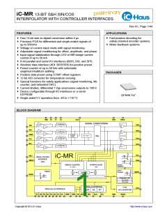
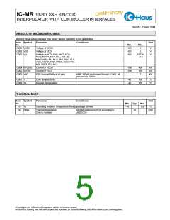
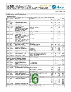
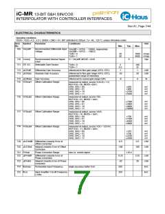
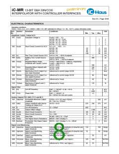
iC-MR 13-BIT S&H SIN/COS
INTERPOLATOR WITH CONTROLLER INTERFACES
Rev A1, Page 4/44
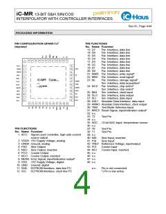
PACKAGING INFORMATION
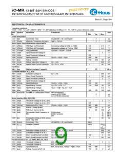
PIN CONFIGURATION QFN48-7x7
(topview)
PIN FUNCTIONS
No. Name Function
13 D7
14 D6
15 D5
16 D4
17 D3
18 D2
19 D1
20 D0
Par. Interface, data line
Par. Interface, data line
Par. Interface, data line
Par. Interface, data line
Par. Interface, data line
Par. Interface, data line
Par. Interface, data line
Par. Interface, data line
21 NWR Par. Interface, write signal*
22 NRD Par. Interface, read signal*
23 NL
Par. Interface, storage signal*
Ser. Interface, data acquisition*
24 NCS Par. Interface, chip select*
Ser. Interface, chip select*
25 MAI
26 SLO Ser. Interface, data output
27 SLI Ser. Interface, data input
Ser. Interface, clock input
28 ASLI Absolute Data Interface, data input
29 AMAO Absolute Data Interface, clock output
30 TMS Test Mode Selection Input
31 NRES Reset Signal, input/indication output*
32 n.c.
33 T2
Test Pin
34 n.c.
35 ADC 12-bit ADC Input, temperature sensor
36 n.c.
PIN FUNCTIONS
No. Name Function
37 T0
38 T1
39 n.c.
40 NSI
41 PSI
Test Pin
Test Pin
1 ACO Signal Level Controller, high-side current
source output
2 VDDA +5V Supply Voltage, analog
3 GNDA Ground, analog
Sine Input, inverted
Sine Input
42 VREF Reference Voltage, input/output
4 PSO Sine Output
5 NSO Sine Output, inverted
6 PCO Cosine Output
43 PCI
44 NCI
45 n.c.
46 n.c.
47 n.c.
48 n.c.
Cosine Input
Cosine Input, inverted
7 NCO Cosine Output, inverted
8 NERR Error Signal, input/indication output*
9 VDD +5V Supply Voltage, digital
10 GND Ground, digital
11 SDA EEPROM Interface, data line I2C
12 SCL EEPROM Interface, clock line I2C
n.c.:
Pin is not connected.
*) Pin is low active.

 ICHAUS [ IC-HAUS GMBH ]