iC-MFN
8-FOLD FAIL-SAFE N-FET DRIVER
Rev A2, Page 9/13
DESCRIPTION OF FUNCTIONS
I(OUTx)
[mA]
3.6
Hi-level output configuration
The device iC-MFN has three adjustable hi-levels for
driving N-channel fets. The configured hi-level is com-
mon to all outputs OUTx and the maxmimum level is
the power supply VB potential. The hi-level configura-
tion inputs are used simultaneous for enabling the hi-
level at the outputs OUTx. The hi-level at exactly one
input EN5, EN10 or ENFS configure the voltage of hi-
level and enable the outputs. If more than one of these
inputs have hi-level the outputs remains disabled. The
hi-level 5 V (configured with EN5 = hi) and 10 V (con-
figured with EN10 = hi) are internally generated by a
voltage reference and regulated. The hi-level VB (con-
figured with ENFS = hi) is an unregulated connection
to VB. In this case the voltage swing depends directly
from the power supply VB.
165
Ω
V(OUTx)−Vr(OUTx)
[V]
−2.5
−2
−1.5
−1
−0.5
0.5
1
1.5
2
2.5
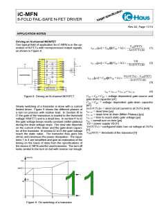
−3
Figure 3: Output characteristic of the regulated
push-pull-output at OUTx
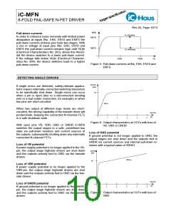
Output characteristic of the lowside transistor
The lowside output transistors at the eight channels
demonstrate a resistive behavior with low voltage
V(OUTx) and behave as a current sink with finite out-
put resistance with higher voltages.
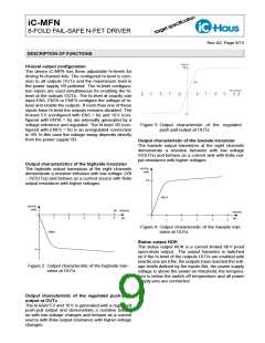
Output characteristics of the highside transistor
The highside output transistors at the eight channels
demonstrate a resistive behavior with low voltage (VB
– V(OUTx)) and behave as a current source with finite
output resistance with higher voltages.
I(OUTx)
[mA]
3.6
400 Ω
I(OUTx)
[mA]
VB −V(OUTx)
V(OUTx)
[V]
1
2
3
4
5
[V]
1
2
3
4
5
Figure 4: Output characteristic of the lowside tran-
sistor at OUTx
−400Ω
Status output NOK
The status output NOK is a current limited 40 V proof
open-drain output. The output transistor is switched
on if the hi-level of the outputs OUTx are enabled with
exactly one pin ENx, the outputs have reached the volt-
age levels defined by the inputs INx, the power supply
voltage is above the power-on threshold, the tempera-
ture is below the switch off temperature and all power
supply pins are connected.
−3
Figure 2: Output characteristic of the highside tran-
sistor at OUTx
Output characteristic of the regulated push-pull-
output at OUTx
The hi-level 5 V and 10 V is generated with a regulated
push-pull output and demonstrate a resistive behav-
ior with low voltage changes and behave as a current
source with finite output resistance with higher voltage
changes.

 ICHAUS [ IC-HAUS GMBH ]