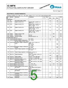
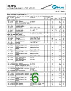
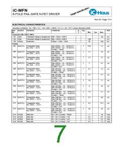
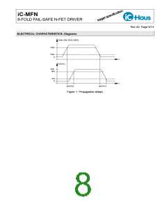
iC-MFN
8-FOLD FAIL-SAFE N-FET DRIVER
Rev A2, Page 10/13
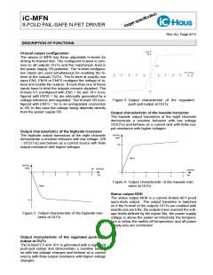
Ipd()
Pull-down currents
V() increasing
In order to enhance noise immunity with limited power
dissipation at inputs INx, EN5, EN10 and ENFS the
pull-down currents at these pins have two stages. With
a rise in voltage at input pins INx, EN5, EN10 und
ENFS the pull-down current remains high until Vt()hi
(Electrical Characteristics No. 203); above this thresh-
old the device switches to a lower pull-down current.
If the voltage falls below Vt()lo (Electrical Character-
istics No. 204), the device switches back to a higher
pull-down current.
Ipd1()
Ipd2()
V() decreasing
Vt()hi
Vt()lo
V()
Figure 5: Pull-down currents at INx, EN5, EN10 and
ENFS
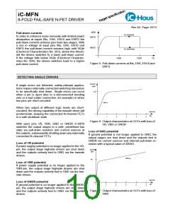
DETECTING SINGLE ERRORS
I(OUTx)
[mA]
If single errors are detected, safety-relevant applica-
tions require externally connected switching transistors
to be specifically shut down. Single errors can occur
when a pin is open (due to a disconnected bonding
wire or a bad solder connection, for example) or when
two pins are short-circuited.
3.6
400 Ω
When two output of different logic levels are short-
circuited, the driving capability of the lowside driver will
predominate, keeping the connected N-channel FETs
in a safe shutdown state.
V(OUTx)
[V]
1
2
3
4
5
Figure 6: Output characeristics at OUTx with loss of
VB, VBR or GNDR
With open pins VB, VBR, GND or GNDR iC-MFN
switches the output stages to a safe, predefined low
state via pull-down resistors and current sources at
the outputs, subsequently shutting down any externally
connected N-channel FETs.
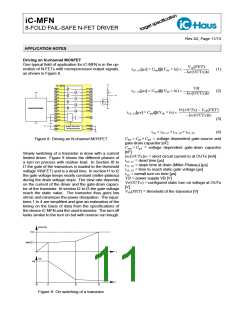
Loss of GND potential
If ground potential is not longer applied to GND, the
output stages are shut down and the outputs tied to
GNDR via current sources and internal pull-down re-
sistors with a typical value of 200 kΩ.
Loss of VB potential
If power supply potential is no longer applied to the VB-
pin, the output stage highside drivers are shut down
and the outputs actively tied to GND via the lowside
drivers.
I(OUTx)
[µA]
200
kΩ
80
Loss of VBR potential
If power supply potential is no longer applied to the
VBR-pin, the output stage highside drivers are shut
down and the outputs actively tied to GND via the low-
side drivers.
V(OUTx)
[V]
Loss of GNDR potential
1
2
3
4
5
If ground potential is no longer applied to the GNDR-
pin, the output stage highside drivers are shut down
and the outputs actively tied to GND via the lowside
drivers.
Figure 7: Output characeristics at OUTx with loss of
GND

 ICHAUS [ IC-HAUS GMBH ]