iC-MFN
8-FOLD FAIL-SAFE N-FET DRIVER
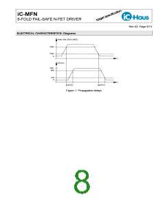
Rev A2, Page 11/13
APPLICATION NOTES
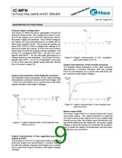
Driving an N-channel MOSFET
One typical field of application for iC-MFN is in the op-
eration of N-FETs with microprocessor output signals,
as shown in Figure 8.
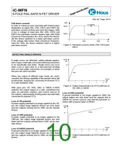
Vth(FET)
(1)
tt0..t1[µs] = Ciss@(Vds = hi)×
−Isc(OUTx)hi
VB
iC−MFN
IN1
IN2
IN3
IN4
IN5
IN6
IN7
IN8
OUT1
OUT2
OUT3
OUT4
OUT5
OUT6
OUT7
OUT8
VB
(2)
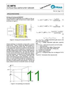
tt1..t2[µs] = Crss@(Vds = hi)×
3.3V
RL
−Isc(OUTx)hi
VD
Microcontroller
Vr(OUTx)−Vth(FET)
−Isc(OUTx)hi
tt2..t3[µs] = Ciss@(Vds = lo)×
EN5
EN10
ENFS
NOK
(3)
VBR
VB
GNDR
GND
VB
Supply, Ground and
Temperature Monitor
ton = tt0..t1 +tt1..t2 +tt2..t3
(4)
Ciss = Cgs +Cgd = voltage dependent gate-source and
gate-drain capacitor [nF]
Figure 8: Driving an N-channel MOSFET
Crss = Cgd = voltage dependent gate-drain capacitor
[nF]
Isc(OUTx)lo = short circuit current lo at OUTx [mA]
tt0..t1 = dead time [µs]
tt1..t2 = slope time at drain (Miller-Plateau) [µs]
tt2..t3 = time to reach static gate voltage [µs]
ton = overall turn on time [µs]
VB = power supply VB [V]
Vr(OUTx) = configured static turn on voltage at OUTx
[V]
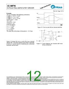
Slowly switching of a transistor is done with a current
limited driver. Figure 9 shows the different phases of
a turn on process with resitive load. In Section t0 to
t1 the gate of the transistors is loaded to the threshold
voltage Vth(FET) and is a dead time. In section t1 to t2
the gate voltage keeps nearly constant (miller-plateau)
during the drain voltage slope. The slew rate depends
on the current of the driver and the gate-drain capaci-
tor of the transistor. In section t2 to t3 the gate voltage
reach the static value. The transistor thus goes low
ohmic and minimizes the power dissipation. The equa-
tions 1 to 4 are simplified and give an estimation of the
timing on the basis of data from the specifications of
the device iC-MFN and the used transistor. The turn off
looks similar to the turn on but with reverse run trough.
Vth(FET) = threshold of the transistor [V]
V(OUTx)
Vr()
Vth(FET)
t
VD
VB
t
t0
t1
t2
t3
Figure 9: On switching of a transistor

 ICHAUS [ IC-HAUS GMBH ]