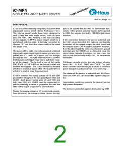
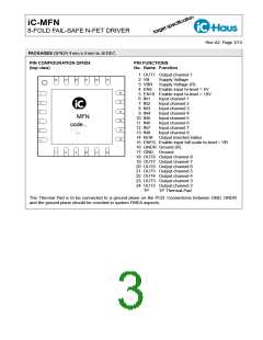
iC-MFN
8-FOLD FAIL-SAFE N-FET DRIVER
Rev A2, Page 4/13
ABSOLUTE MAXIMUM RATINGS
Beyond these values damage may occur; device operation is not guaranteed.
Item Symbol
No.
Parameter
Conditions
Unit
Min.
-0.3
-0.3
-0.3
-0.3
-0.3
-0.3
-0.3
-10
Max.
G001 VB, VBR
G002 V()
Supply Voltage
40
40
V
V
Voltage at OUT1...8, NOK
Voltage at IN1...8, EN5, EN10, ENFS
G003 V()
40
V
G004 V(GNDR) Voltage at GNDR referenced to GND
0.3
0.3
0.3
0.3
10
V
G005 V(GND)
G006 V(VBR)
G007 V(VB)
G008 Imx()
Voltage at GND referenced to GNDR
Voltage at VBR referenced to VB
Voltage at VB referenced to VBR
V
V
V
Current in OUT1...8, NOK, IN1...8,
EN5, EN10, ENFS
mA
G009 Imx()
G010 Imx()
G011 Vd()
G012 Tj
Current in VB, VBR
-10
-80
80
10
mA
mA
kV
°C
Current in GND, GNDR
ESD susceptibility at all pins
Operating Junction Temperature
Storage Temperature Range
HBM 100 pF discharged through 1.5 kΩ
2
-40
-55
140
125
G013 Ts
°C
THERMAL DATA
Operating Conditions: VB = VBR = 4.5. . . 40 V, GND = GNDR = 0 V
Item Symbol
No.
Parameter
Conditions
Unit
Min. Typ. Max.
T01 Ta
Operating Ambient Temperature Range
Thermal Resistance Chip/Ambient
-40
125
75
°C
T02 Rthja
SMD assembly, no additional cooling areas.
K/W
All voltages are referenced to ground unless otherwise stated.
All currents into the device pins are positive; all currents out of the device pins are negative.

 ICHAUS [ IC-HAUS GMBH ]