iC-MFN
8-FOLD FAIL-SAFE N-FET DRIVER
Rev A2, Page 3/13
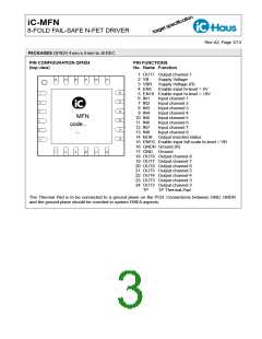
PACKAGES QFN24 4 mm x 4 mm to JEDEC
PIN CONFIGURATION QFN24
(top view)
PIN FUNCTIONS
No. Name Function
1 OUT1 Output channel 1
23
22
24
21
20
19
2 VB
3 VBR Supply Voltage (R)
4 EN5 Enable input hi-level = 5V
5 EN10 Enable input hi-level = 10V
Supply Voltage
18
17
16
15
14
13
1
2
6 IN1
7 IN2
8 IN3
Input channel 1
Input channel 2
Input channel 3
Input channel 4
Input channel 5
Input channel 6
Input channel 7
Input channel 8
3
9 IN4
MFN
code...
...
10 IN5
11 IN6
12 IN7
13 IN8
4
5
14 NOK Output inverted status
15 ENFS Enable input full scale hi-level = VB
16 GNDR Ground (R)
6
17 GND Ground
8
9
10
12
7
11
18 OUT8 Output channel 8
19 OUT7 Output channel 7
20 OUT6 Output channel 6
21 OUT5 Output channel 5
22 OUT4 Output channel 4
23 OUT3 Output channel 3
24 OUT2 Output channel 2
TP
TP Thermal-Pad
The Thermal Pad is to be connected to a ground plane on the PCB. Connections between GND, GNDR
and the ground plane should be conciled to system FMEA aspects.

 ICHAUS [ IC-HAUS GMBH ]