iC-JX
16-FOLD 24 V HIGH-SIDE DRIVER WITH µC INTERFACE
Rev C1, Page 10/36
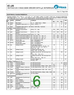
ELECTRICAL CHARACTERISTICS
Operating conditions: VCC = VDD = 3 ... 5.5 V, VBy = 12 ... 36 V, GNDA = GNDD = 0 V, RSET = 10 kΩ ±1% . All inputs on defined logic
states (high or low), Tj = -40 ... 125 °C unless otherwise stated. Functionality and parameters beyond operating conditions (for example
w.r. to independent voltage supplies) are to be verified within the individual application by FMEA methods.
Item Symbol
No.
Parameter
Conditions
Unit
Min.
Typ.
Max.
K02 Vt()lo
Threshold voltage Low at
Schmitt-Trigger-Inputs
D0...7 with input function
0.8
V
NCS, NWR, NRD, A0...4, NRES,
CLK, BLFQ, D0...7, NSP, POE
K03 Vt()hys
Schmitt-Trigger-Hysteresis at
Vt()hys = Vt()hi - Vt()lo;
150
mV
inputs NCS, NWR, NRD, A0...4, D0...7 mit Eingangsfunktion
NRES, CLK, BLFQ, D0...7, NSP,
POE
K04 Vs()hi
K05 Vs()lo
K06 Ipd()
Saturation voltage high
an NINT, Dx
Vs()hi = VDD - V( );
I( ) = -4 mA
0.8
0.49
70
V
V
Saturation voltage low
an NINT, Dx
I( ) = 4 mA
Pull Down current sources at
A0...4, NRES, CLK, BLFQ,
D0...7, POE
V() = 1V .. VDD
2
µA
K07 Ipu()
Pull Up current sources at NSP, V() = 0V .. VDD - 1 V
NCS, NWR, NRD
-70
2
6
µA
µs
ns
ns
ns
K08 tp(POE-
IOx)
Delay time output enable:
POE to IOx disabled
RL = 240 Ω... 1 kΩ, POE: hi → lo
to V(IOx) < 80 % (VBy - Vs(IOx)hi)
K09 tw()lo
Permissible pulse width for en-
able/disable at POE
600
200
K10 tw()
Permissible burst pulse width at
POE
100
K11 tmin()nres minimum duration for reset at
NRES
Frequency BLFQ, CLK
P01 td()
P02 td()
maximum frequency at CLK
maximum frequency at BLFQ
TBD
TBD
MHz
MHz
Characteristics: Diagrams
Figure 1: DC load
Figure 2: Pulse load

 ICHAUS [ IC-HAUS GMBH ]