iC-GF
TRANSCEIVER
Rev C1, Page 21/26
REGISTERS
Configuration overview
OVL(1:0) and UVD(1:0) are set to high during the re-
The configuration bytes are readable and writeable, spective error condition and stay high for least 35 ms
with the exception of the IND bit (adr 0x00). The di- after the condition has been removed (Electrical Char-
agnostic register is read only. After reading, the bits acteristics Nos. 302, 405). Tables 27, 28 and 29 show
CFED, INITRAM and WUD are reset. The bits OVT, an overview of the registers, accessible in SPI mode.
Register Address Bits Default Description
DUTY
ENCFD
ENOD
ENPUD
ENRND
ENSCR
FCFG
FCFI
0x03
0x02
0x01
0x01
0x02
0x02
0x02
0x02
0x00
0x03
0x01
0x03
0x00
0x00
0x01
0x01
0x01
0x00
0x02
3:2
7
10 Duty cycle configuration for overload detection
0
1
1
1
0
Enable logging of changes at CFI
Enable Open-Drain output at RX pin
Enable pull-up/down current at CFI pin
Enable spread spectrum oscillator
Enable communication requests
0
3
4
6
3:2
1:0
7
10 Filter configuration for TX and OEN
01 Filter configuration for CFI
IND
R/O CFI status (independent of POL), r/o
00 Switching channel inversion
INV
5:4
1
INVPUD
NEXC
OEN
0 Invert pull-up/down configuration at CFI
1:0
3:2
1:0
2
11 Enable excitation current for capacitive loads
11 Switching channel enable
OUTD
POL
00 Output data for the switching channels
0
Polarity inversion at CFI
QCFG1
QCFG2
TXEN
SCR2
5:4
7:6
5:4
5
11 Switching channel 1 configuration
11 Switching channel 2 configuration
01 Channel control select (register or pin)
0
Communication request channel selection
Table 27: Overview of the configuration registers
Register Address Bits Description
INITR
SCR
0x04
0x04
0x04
0x04
0x04
0x04
0x04
0x04
0
1
2
3
4
5
6
7
Register reset
Communication request acknowledged
Change detection at CFI
Overtemperature
CFED
OVT
OVL(0)
OVL(1)
UVD(0)
UVD(1)
Overload Channel 1
Overload Channel 2
Undervoltage VCC resp. VCC3
Undervoltage VBO
Table 28: Overview of the diagnostic register (read only)
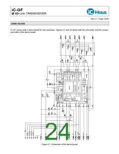
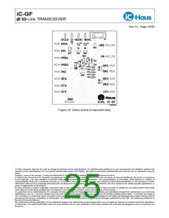
OVERVIEW
Adr
0x00
0x01
0x02
0x03
0x04
Bit 7
Bit 6
Bit 5
Bit 4
Bit 3
Bit 2
Bit 1
Bit 0
IND
TXEN(1:0)
QCFG1(1:0)
SCR2 ENRND
OEN(1:0)
OUTD(1:0)
QCFG2(1:0)
ENCFD ENSCR
ENPUD
POL
INVPUD
ENOD
FCFG(1:0)
DUTY(1:0)
FCFI(1:0)
NEXC(1:0)
SCR INITR
INV(1:0)
OVL(1:0)
UVD(1:0)
OVT
CFED
Table 29: Register layout

 ICHAUS [ IC-HAUS GMBH ]