IBM3009K2672
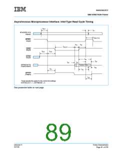
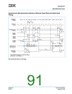
IBM SONET/SDH Framer
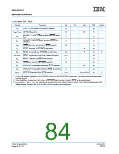
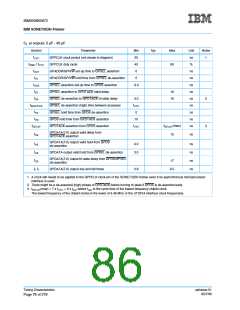
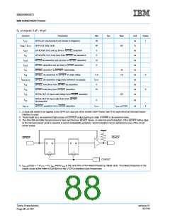
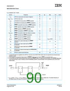
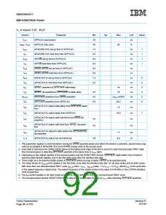
C at outputs: 5 pF - 40 pF
L
Symbol
Parameter
Min
20
40
0
Typ
Max
60
Unit
ns
%
Notes
1
tCYC
tPWH / tCYC
tSU1
GPPCLK clock period (not shown in diagram)
GPPCLK duty cycle
GPADDR(13:0) set-up time to GPSEL assertion
GPADDR(13:0) hold time from GPSEL de-assertion
GPRD de-assertion set-up time to GPSEL assertion
GPSEL assertion set-up time to GPWR assertion
GPSEL assertion to GPRDY valid delay
ns
ns
ns
ns
ns
ns
ns
ns
ns
ns
tH1
0
tSU2
10
0
tSU3
tD1
16
16
tD2
GPSEL de-assertion to GPRDY tri-state delay
GPSEL de-assertion (high) time between accesses
GPSEL hold time from GPWR de-assertion
GPWR hold time from GPRDY assertion
GPDATA(7:0) input valid delay from GPWR assertion
4.0
2
3
tINACTIVE
tH2
tCYC
0
tH3
10
tD3
20
GPDATA(7:0) input valid hold from GPWR
de-assertion
tH4
0
ns
ns
tDELAY
tCYC
tDELAY(max)
GPRDY assertion from GPWR assertion
4
1. A clock still needs to be applied to the GPPCLK clock pin of the SONET/SDH framer even if an asynchronous microprocessor
interface is used.
2. There might be a de-asserted (high) phase of GPDRDY before turning tri-state if GPWR is de-asserted early.
3. The Intel 286 and 386 microprocessors have synchronous READY inputs, so external synchronization of the GPRDY falling edge
to the microprocessor clock is required to avoid metastability problems. Synchronization can be achieved by use of the circuit
shown below:
READY
GPRDY
D
Q
D
Q
CLKOUT
4. tDELAY(max) = 7 x tCYC + 6 x tmin where tmin is the cycle time of the lowest-frequency chiplet clock. The lowest frequency of the
chiplet clocks is the lower of 6.48 MHz or the UTOPIA interface clock frequencies.
Timing Characteristics
Page 80 of 279
ssframer.01
8/27/99

 IBM [ IBM ]