IBM3009K2672
IBM SONET/SDH Framer
• STM-16/STM-4 or STS-48/STS-12 mode
- K1, K2 plus the New APS indication bit, and Line RDI, are processed only for the first STM-1/STS-3c
in the SONET/SDH framer that corresponds to STM-4/STS-12 1.
- Line REI is processed only for the third STM-1 in the SONET/SDH framer that corresponds to STM-
4/STS-12 1. The receive B2 errors from the twelve B2 bytes received from the line and the expansion
port are summed by macro 3 of the SONET/SDH framer that corresponds to STM-4/STS-12 1 and
are transferred to a mating SONET/SDH framer which then outputs this value to its line output via the
transmit M1 byte. The M1 byte is located in row 9 column 51 (the third A2 byte is also in column 51) of
the STM-16/STS-48 frame.
- K3 is processed for all 4 VC-4s of each SONET/SDH framer.
- G1 is processed for all 4 VC-4 of each SONET/SDH framer.
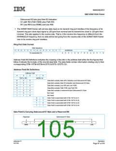
Alarm bits are provided to indicate that an alarm was asserted in the corresponding alarm bit in bit location 8
of the data field; see Ring Port Data Format on page 97. If the RING control bit is set to ’0’, the SONET/SDH
framer will ignore the ring port inputs and force its ring port outputs to a stable logic level. The loss of ring data
(AIP_DLoss bit in OT#IRQ2 #=1-4) and loss of ring clock (LTRC) event bits will also be disabled. This means
that they will not be affected by TXRINGD and TXRINGCLK.
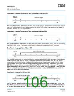
The K1, K2, and K3 bytes for all four STM-1/STS-3cs that are received at the ring port inputs are stored in
registers in the SONET/SDH framer for access by the local microprocessor provided that the RING control bit
is set to a ‘1’. The K1, K2, and K3 bytes are updated each time they are received at the transmit ring port
inputs. The K1, K2, and K3 bytes are stored in the OT#Stat3-5 registers, where # = 1, 2, 3, 4. When the RING
control bit is set to a ’0’, the SONET/SDH framer does not update the K1 - K3 register locations from the
transmit ring port. Instead, these values are derived from the local receive SONET/SDH line. Each time the
SONET/SDH framer receives a Line RDI Indication on its transmit ring port input the SONET/SDH framer will
transmit a Line RDI at its transmit line output.
When the RING control bit is set to ‘1’ and the SONET/SDH framer is set up to process four individual STM-
1/STS-3cs, the Line REI received at the transmit ring port input is inserted into the M1 byte of the correspond-
ing STM-1/STS-3c macro in the outgoing SONET/SDH stream of the SONET/SDH framer. When the
SONET/SDH framer is set up to process an STM-4/4c or an STS-12/12c, the SONET/SDH framer will insert
the Line REI count received at its ring port for macro 3 into the M1 byte for macro 3. When the SONET/SDH
framer is set up for STM-16/STS-48 mode, macro 3 of the SONET/SDH framer that corresponds to STM-4/4c
or STS-12/12c 1 will add the B2 errors indicated on its expansion port to the Line REI that it gets from the ring
port and insert that count into the outgoing M1 byte of macro 3. The Line REIs due to B2 errors received from
the receive line will not be inserted into the outgoing M1 byte(s) of their corresponding local STM-1/STS-3cs.
No data is lost due to clock tolerance offsets between the TXRINGCLK signal and the SONET/SDH transmit
clock of the same SONET/SDH framer.
When the RING control bit is set to ‘1’, the Path FEBE and RDI inputs at the transmit ring port are inserted
into the G1 byte of the corresponding VC-4 (or VC-4-4c) in the outgoing SONET/SDH stream of the
SONET/SDH framer. Locally detected B3 errors and alarms will not have any effect on the transmit G1 bytes.
It is important to note that no POH processing is performed by the SONET/SDH framer when the Telecom
Bus interface is used. This includes the ring port. When the Telecom Bus interface is used, all Path FEBE and
RDI values must be handled by the path layer device connected to the Telecom Bus.
When the RING control bit is set to ’0’, the G1 byte values in the TXRINGD stream are ignored by the
SONET/SDH framer. Instead, the transmit G1 byte(s) is(are) determined by the locally-detected B3 errors
and alarms, provided that Telecom Bus mode is not activated.
Operation
ssframer.01
8/27/99
Page 100 of 279

 IBM [ IBM ]