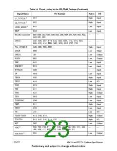
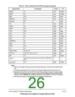
Note:
1. These are test signals for factory use only and must be pulled up to OVdd for normal operation.
2. OVdd inputs supply power to the I/O drivers and Vdd inputs supply power to the processor core.
3. Internally tied to GND in the 255 CBGA package to indicate to the power supply that a low-voltage pro-
cessor is present. This is NOT a supply pin.
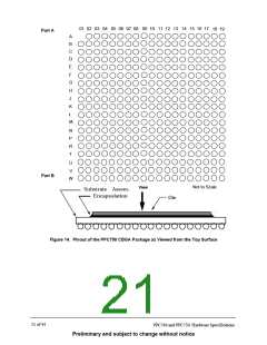
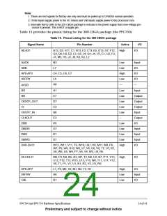
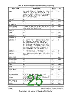
Table 15 provides th e pin ou t listin g for th e 360 CBGA package (th e PPC750).
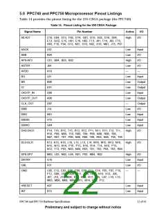
Table 15. Pinout Listing for the 360 CBGA package
Signal Name
A0-A31
Pin Number
Active
I/O
A13, D2, H11, C1, B13, F2, C13, E5, D13, G7, F12, High
G3, G6, H2, E2, L3, G5, L4, G4, J4, H7, E1, G2, F3,
J7, M3, H3, J2, J6, K3, K2, L2
I/O
AACK
N3
Low
Low
High
Low
—
Input
I/O
I/O
I/O
—
ABB
L7
AP0-AP3
ARTRY
C4, C5, C6, C7
L6
A8
AVDD
BG
H1
E7
D7
C2
B8
E3
K5
G1
K1
D1
Low
Low
Low
Low
Low
--
Input
Output
Output
Output
Input
Output
I/O
BR
CKSTP_OUT
CI
CKSTP_IN
CLKOUT
DBB
Low
Low
Low
Low
High
DBDIS
DBG
Input
Input
Input
I/O
DBWO
DH0-DH31
W12, W11, V11, T9, W10, U9, U10, M11, M9, P8,
W7, P9, W9, R10, W6, V7, V6, U8, V9, T7, U7, R7,
U6, W5, U5, W4, P7, V5, V4, W3, U4, R5
DL0-DL31
M6, P3, N4, N5, R3, M7, T2, N6, U2, N7, P11, V13, High
U12, P12, T13, W13, U13, V10, W8, T11, U11, V12,
V8, T1, P1, V1, U1, N1, R2, V3, U3, W2
I/O
DP0-DP7
DRTRY
GBL
L1, P2, M2, V2, M1, N2, T3, R1
High
Low
Low
I/O
H6
B1
Input
I/O
PPC740 and PPC750 Hardware Specifications
24 of 43
Preliminary and subject to change without notice

 IBM [ IBM ]