4.0 PPC740 and PPC750 Microprocessor Pin Assignments
Th e followin g section s con tain th e pin ou t diagram s for th e PPC740 an d PPC750. IBM
offers two ceram ic ball grid array (BGA) packages: a 255 CBGA (th e PPC740) an d a 360
CBGA (th e PPC750).
Figu re 13 (in part A) sh ows th e pin ou t of th e 255 CBGA package as viewed from th e top
su rface. Part B sh ows th e side profile of th e 255 CBGA package to in dicate th e direc-
tion of th e top su rface view.
01 02 03 04 05 06 07 08 09 10 11 12 13 14 15 16
Part A
A
B
C
D
E
F
G
H
J
K
L
M
N
P
R
T
Not to Scale
Part B
View
Su bstrate Assem -
En capsu lation
Die
Figure 13. Pinout of the PPC740 BGA Package as Viewed from the Top Surface
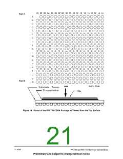
Figu re 14 (in part A) sh ows th e pin ou t of th e 360 CBGA package as viewed from th e top
su rface. Part B sh ows th e side profile of th e 360 CBGA package to in dicate th e direc-
tion of th e top su rface view.
PPC740 and PPC750 Hardware Specifications
20 of 43
Preliminary and subject to change without notice

 IBM [ IBM ]