IBM PowerPC 403GCX
Package Thermal Specifications
Operating Conditions
The 403GCX can interface to either 3V or 5V
technologies. The range for supply voltages is
specified for five-percent margins relative to a
nominal 3.3V power supply, or +/- 100mV at 3.4
Volt supply with 403GCX-3JC80A and 403GCX-
3BC80A.
The 403GCX is designed to operate within the
case temperature range from -40°C to 120°C.
Thermal resistance values are shown in Table 7:
Table 7. Thermal Resistance (°C/Watt)
Airflow-ft/min (m/
Device operation beyond the conditions specified
in Table 9 is not recommended. Extended opera-
tion beyond the recommended conditions may
affectdevice reliability:
sec)
Parameter
0
(0)
100
(0.51) (1.02)
200
2
2
2
θ
θ
JC Junction to case
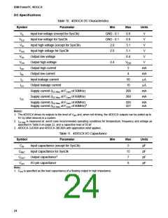
Table 9. Operating Conditions
CA Case to ambient
Sym
bol
Parameter
Min Max Unit
PQFP (no heatsink)
37.2
30
31.6
29.8
PBGA (no heatsink)5
VDD Supply voltage:
403GCX-3JC50/66/80
Notes:
3.14 3.47
3.3 3.5
3.14 3.47
V
1. Case temperature Tm is measured at top center of
C
403GCX-3JC80A
case surface with device soldered to circuit board.
403GCX-3BC50/66/80
403GCX-3BC80A
2. Tm = Tm – P×θCA, where Tm is ambient tem-
A
C
A
perature.
3.3
3.5
3. TmCMax = TmJMax – P×θJC, where TmJMax is maxi-
mum junction temperature and P is power con-
sumption.
4. The above assumes that the chip is mounted on a
card with at least one signal and two power planes.
1
Clock frequency :
FC
403GCX-3JC50/3BC50
403GCX-3JC66/3BC66
403GCX-3JC80/3BC80
403GCX-3JC80A/3BC80A
24
24
24
24
25 MHz
33
40
40
ELECTRICAL SPECIFICATIONS
Absolute Maximum Ratings
TmC Case temperature
403GCX-3JC50/66/80/80A -40
85
85
°C
403GCX-3BC50/66/80/80A -40
The absolute maximum ratings in Table 8 below
are stress ratings only. Operation at or beyond
these maximum ratings may cause permanent
damage to the device.
Note:
1. These frequencies do not account for T . See
CS
Table 12.
Power Considerations
Power dissipation is determined by operating fre-
quency, temperature, and supply voltage, as well
as external source/sink current requirements.
Typical power dissipation is 0.34 W at 25/50
MHz, 0.42 W at 33/66 MHz, or 0.51 W at 40/80
MHz, TmC = 55 °C, and VCC = 3.3 V, with an
average 50pF capacitive load. Typical power dis-
sipation is 0.54w for 403GCX-3JC80A and
403GCX-3BC80A. TmC = 55 °C, and VCC = 3.3
V, with an average 50pF capacitive load. Derat-
ing curves are provided in the section, "Output
Derating for Capacitance and Voltage," on page
33.
Table 8. 403GCX Maximum Ratings
Parameter
Maximum Rating
Supply voltage with
respect to GND
-0.5V to +3.8V
Voltage on other pins with
respect to GND
-0.5V to +5.5V
-40°C to +120°C
-65°C to +150°C
Case temperature under
bias
Storage temperature
22

 IBM [ IBM ]