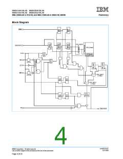
IBM0418A81BLAB IBM0436A81BLAB
IBM0418A41BLAB IBM0436A41BLAB
Preliminary
8Mb (256Kx36 & 512x18) and 4Mb (128Kx36 & 256Kx18) SRAM
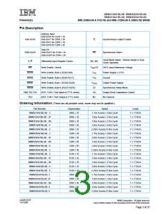
Recommended DC Operating Conditions (TA = 0 to +85°C)
Parameter
Symbol
Min.
2.5 - 5%
1.4
Typ.
2.5
Max.
2.5 + 5%
1.9
Units
V
Notes
1
V
Supply Voltage
DD
V
1
Output Driver Supply Voltage
Input High Voltage
1.5, 1.8
—
V
DDQ
V
V
+0.1
V
DDQ
+ 0.3
- 0.1
1, 2
1, 3
1, 6
1, 4
1, 5
1
V
IH
REF
V
V
REF
Input Low Voltage
-0.3
—
V
IL
V
Input Reference Voltage
Clocks Signal Voltage
0.68
-0.3
0.1
0.90
—
0.95
V
REF
V
V
V
+ 0.3
+ 0.6
V
IN - CLK
DIF - CLK
CM - CLK
DDQ
DDQ
V
V
Differential Clocks Signal Voltage
Clocks Common Mode Voltage
—
V
0.55
—
0.90
V
1. All voltages referenced to V . All V , V
, and V pins must be connected.
SS
SS
DD
DDQ
2. V (Max)DC = V
+ 0.3 V, V (Max)AC = V
+ 0.85 V (pulse width ≤ 4.0ns).
IH
DDQ
IH
DDQ
3. V (Min)DC = -0.3 V, V (Min)AC = -1.5 V (pulse width ≤ 4.0ns).
IL
IL
4. V
5. V
specifies the maximum allowable DC excursions of each differential clock (K, K).
IN-CLK
specifies the minimum Clock differential voltage required for switching.
DIF-CLK
6. Peak to Peak AC component superimposed on V
may not exceed 5% of V
REF.
REF
crrh2519.07
12/13/00
©IBM Corporation. All rights reserved.
Use is further subject to the provisions at the end of this document.
Page 7 of 25

 IBM [ IBM ]