IBM0418A81BLAB IBM0436A81BLAB
IBM0418A41BLAB IBM0436A41BLAB
Preliminary
8Mb (256Kx36 & 512x18) and 4Mb (128Kx36 & 256Kx18) SRAM
AC Input Characteristics
Item
Symbol
Min
V + 0.4
REF
Max
Notes
3
V
(ac)
(ac)
(ac)
(ac)
AC Input Logic High
IH
V
V
- 0.4
AC Input Logic Low
3
2
1
IL
REF
V
V
Clock Input Differential Voltage
0.7
DIF
V
Peak to Peak ac Voltage
5% V
(dc)
REF
REF
REF
1. The peak to peak AC component superimposed on V
may not exceed 5% of the DC component of V
REF.
REF
2. Performance is a function of V and V levels to clock inputs.
IH
IL
3. See the AC Input Definition figure below.
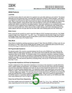
AC Input Definition
V
(ac)
IH
V
REF
V
(ac)
IL
Programmable Impedance Output Driver DC Electrical Characteristics
(TA = 0 to +85°C, VDD = 2.5V -5%, +5%, VDDQ = 1.8 V)
Parameter
Output “High” Level Voltage
Output “Low” Level Voltage
Symbol
Min.
Max.
Units
V
Notes
1, 3
V
V
/ 2
V
OH
DDQ
DDQ
V
V
V / 2
DDQ
2, 3
V
OL
SS
RQ
VDDQ
------------------
2
⁄
-------- + 5
5
1. I
2. I
=
=
± 15% @ V = V / 2 For: 175Ω ≤ RQ ≤ 350Ω.
DDQ
OH
OH
VDDQ
------------------
2
RQ
--------
⁄
± 15% @ V = V
/ 2 For: 175Ω ≤ RQ ≤ 350Ω.
DDQ
OL
OL
5
3. Parameter tested with RQ = 250Ω and V
= 1.8 V.
DDQ
crrh2519.07
12/13/00
©IBM Corporation. All rights reserved.
Use is further subject to the provisions at the end of this document.
Page 9 of 25

 IBM [ IBM ]