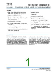
IBM0418A81BLAB IBM0436A81BLAB
IBM0418A41BLAB IBM0436A41BLAB
Preliminary
8Mb (256Kx36 & 512x18) and 4Mb (128Kx36 & 256Kx18) SRAM
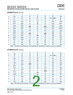
Pin Description
Address Input
SA0-SA18 for 512K x 18
SA0-SA17 for 256K x 36
SA0-SA17 for 256K x 18
SA0-SA16 for 128K x 36
SA0-SA18
G
Asynchronous Output Enable
Synchronous Select
Data I/O
DQ0-DQ17 for 512K x 18
DQ0-DQ35 for 256K x 36
DQ0-DQ35
K, K
SS
Clock Mode Inputs - Selects Single or Dual
Clock Operation.
Differential Input Register Clocks
M1, M2
V
(2)
SW
Write Enable, Global
HSTL Input Reference Voltage
Power Supply (+2.5V)
Ground
REF
V
SBWa
SBWb
Write Enable, Byte a (DQ0-DQ8)
Write Enable, Byte b (DQ9-DQ17)
DD
V
SS
V
SBWc
SBWd
Write Enable, Byte c (DQ18-DQ26)
Write Enable, Byte d (DQ27-DQ35)
IEEE 1149.1 Test Inputs (LVTTL levels)
IEEE 1149.1 Test Output (LVTTL level)
Output Power Supply
Synchronous Sleep Mode
Output Driver Impedance Control
No Connect
DDQ
ZZ
ZQ
NC
TMS,TDI,TCK
TDO
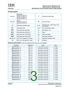
Ordering Information (These are all possible sorts; some may not be qualified.)
Part Number
Organization
256K x 18
256K x 18
256K x 18
256K x 18
256K x 18
128K x 36
128K x 36
128K x 36
128K x 36
128K x 36
512K x 18
512K x 18
512K x 18
512K x 18
512K x 18
256K x 36
256K x 36
256K x 36
256K x 36
256K x 36
Speed
Leads
IBM0418A41BLAB - 3
IBM0418A41BLAB - 3F
IBM0418A41BLAB - 3N
IBM0418A41BLAB - 4
IBM0418A41BLAB - 5
IBM0436A41BLAB - 3
IBM0436A41BLAB - 3F
IBM0436A41BLAB - 3N
IBM0436A41BLAB - 4
IBM0436A41BLAB - 5
IBM0418A81BLAB - 3
IBM0418A81BLAB - 3F
IBM0418A81BLAB - 3N
IBM0418A81BLAB - 4
IBM0418A81BLAB - 5
IBM0436A81BLAB -3
IBM0436A81BLAB -3F
IBM0436A81BLAB - 3N
IBM0436A81BLAB -4
IBM0436A81BLAB -5
1.7ns Access / 3.0ns Cycle
1.8ns Access / 3.3ns Cycle
1.8ns Access / 3.7ns Cycle
2.0ns Access / 4.0ns Cycle
2.25ns Access /5.0ns Cycle
1.7ns Access / 3.0ns Cycle
2.0ns Access / 3.3ns Cycle
1.8ns Access / 3.7ns Cycle
2.0ns Access / 4.0ns Cycle
2.25ns Access /5.0ns Cycle
1.7ns Access / 3.0ns Cycle
1.8ns Access / 3.3ns Cycle
1.8ns Access / 3.7ns Cycle
2.0ns Access / 4.0ns Cycle
2.25ns Access /5.0ns Cycle
1.7ns Access / 3.0ns Cycle
1.8ns Access / 3.3ns Cycle
1.8ns Access / 3.7ns Cycle
2.0ns Access / 4.0ns Cycle
2.25ns Access /5.0ns Cycle
7 x 17 BGA
7 x 17 BGA
7 x 17 BGA
7 x 17 BGA
7 x 17 BGA
7 x 17 BGA
7 x 17 BGA
7 x 17 BGA
7 x 17 BGA
7 x 17 BGA
7 x 17 BGA
7 x 17 BGA
7 x 17 BGA
7 x 17 BGA
7 x 17 BGA
7 x 17 BGA
7 x 17 BGA
7 x 17 BGA
7 x 17 BGA
7 x 17 BGA
crrh2519.07
12/13/00
©IBM Corporation. All rights reserved.
Use is further subject to the provisions at the end of this document.
Page 3 of 25

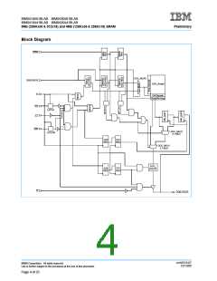
 IBM [ IBM ]