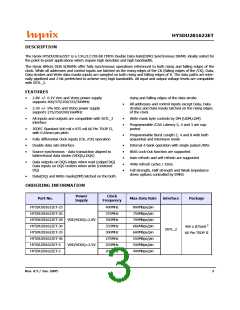
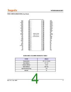
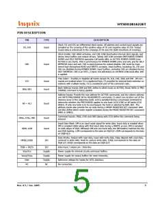
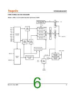
HY5DU281622ET
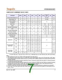
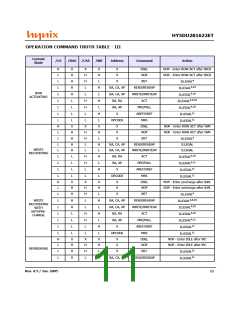
SIMPLIFIED COMMAND TRUTH TABLE
A10/
AP
Command
CKEn-1
CKEn
CS
RAS
CAS
WE
ADDR
BA
Note
Extended Mode Register Set
Mode Register Set
Device Deselect
No Operation
H
H
X
X
L
L
L
L
L
L
L
L
OP code
OP code
1,2
1,2
H
L
X
H
L
X
H
H
X
H
H
H
H
H
X
X
X
X
1
Bank Active
L
RA
V
V
1
1
Read
L
H
L
L
L
L
H
H
L
L
L
H
L
CA
CA
X
Read with Autoprecharge
Write
1,3
1
H
H
X
X
V
Write with Autoprecharge
Precharge All Banks
Precharge selected Bank
Read Burst Stop
Auto Refresh
H
H
L
1,4
1,5
1
X
V
H
L
H
H
H
X
H
L
L
L
H
L
H
L
L
H
H
X
H
X
H
X
H
X
V
X
X
1
1
Entry
L
L
L
1
Self Refresh
Exit
H
L
X
H
X
H
X
H
X
V
X
H
X
H
X
H
X
V
X
X
X
L
H
L
H
L
1
H
L
1
1
1
1
1
1
1
Entry
Precharge Power
Down Mode
H
L
Exit
H
H
L
Entry
H
L
L
Active Power
Down Mode
Exit
H
X
( H=Logic High Level, L=Logic Low Level, X=Don’t Care, V=Valid Data Input, OP Code=Operand Code, NOP=No Operation )
Note :
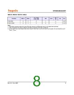
1. UDM, LDM states are Don’t Care. Refer to below Write Mask Truth Table.(note 6)
2. OP Code(Operand Code) consists of A0~A11 and BA0~BA1 used for Mode Register setting during Extended MRS or MRS. Before
entering Mode Register Set mode, all banks must be in a precharge state and MRS command can be issued after tRP period from
Prechagre command.
3. If a Read with Auto-precharge command is detected by memory component in CK(n), then there will be no command presented
to activate bank until CK(n+BL/2+tRP).
4. If a Write with Auto-precharge command is detected by memory component in CK(n), then there will be no command presented
to activate bank until CK(n+BL/2+1+tDPL+tRP). Last Data-In to Prechage delay(tDPL) which is also called Write Recovery
Time(tWR) is needed to guarantee that the last data have been completely written.
5. If A10/AP is High when Precharge command being issued, BA0/BA1 are ignored and all banks are selected to be precharged.
6. In here, Don’t Care means logical value only, it doesn’t mean ’Don’t care for DC level of each signals’. DC level should be out of
V
IHmin ~ VILmax
Rev. 0.5 / Jan. 2005
7

 HYNIX [ HYNIX SEMICONDUCTOR ]