HY5DU281622ET
DESCRIPTION
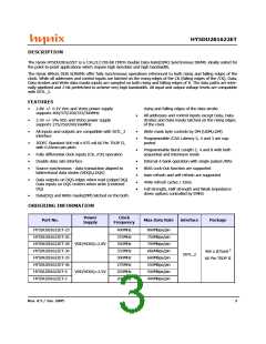
The Hynix HY5DU281622ET is a 134,217,728-bit CMOS Double Data Rate(DDR) Synchronous DRAM, ideally suited for
the point-to-point applications which require high densities and high bandwidth.
The Hynix 8Mx16 DDR SDRAMs offer fully synchronous operations referenced to both rising and falling edges of the
clock. While all addresses and control inputs are latched on the rising edges of the CK (falling edges of the /CK), Data,
Data strobes and Write data masks inputs are sampled on both rising and falling edges of it. The data paths are inter-
nally pipelined and 2-bit prefetched to achieve very high bandwidth. All input and output voltage levels are compatible
with SSTL_2.
FEATURES
•
•
•
•
2.8V +/- 0.1V VDD and VDDQ power supply
supports 400/375/350/333/300MHz
rising and falling edges of the data strobe
•
All addresses and control inputs except Data, Data
strobes and Data masks latched on the rising edges
of the clock
2.5V +/- 5% VDD and VDDQ power supply
supports 275/250/200/166MHz
All inputs and outputs are compatible with SSTL_2
interface
•
•
Write mask byte controls by DM (UDM,LDM)
Programmable /CAS Latency 5, 4 and 3 are sup-
ported
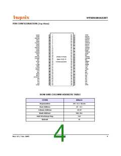
JEDEC Standard 400 mil x 875 mil 66 Pin TSOP II,
with 0.65mm pin pitch
•
Programmable Burst Length 2, 4 and 8 with both
sequential and interleave mode
•
•
•
Fully differential clock inputs (CK, /CK) operation
Double data rate interface
•
•
•
•
•
Internal 4 bank operation with single pulsed /RAS
tRAS Lock-Out function are supported
Auto refresh and self refresh are supported
4096 refresh cycles / 32ms
Source synchronous - data transaction aligned to
bidirectional data strobe (UDQS,LDQS)
•
Data outputs on DQS edges when read (edged DQ)
Data inputs on DQS centers when write (centered
DQ)
Full strength, Half strength and Weak Impedance
driver options controlled by EMRS
•
Data(DQ) and Write masks(DM) latched on the both
ORDERING INFORMATION
Power
Clock
Frequency
Part No.
Supply
Max Data Rate
interface
Package
HY5DU281622ET-25
400MHz
375MHz
350MHz
333MHz
300MHz
275MHz
250MHz
200MHz
800Mbps/pin
750Mbps/pin
700Mbps/pin
666Mbps/pin
600Mbps/pin
550Mbps/pin
500Mbps/pin
400Mbps/pin
HY5DU281622ET-26
HY5DU281622ET-28 VDD/VDDQ=2.8V
HY5DU281622ET-30
400 x 875mil 2
66 Pin TSOP II
SSTL_2
HY5DU281622ET-33
HY5DU281622ET-36
HY5DU281622ET-4
HY5DU281622ET-5
VDD/VDDQ=2.5V
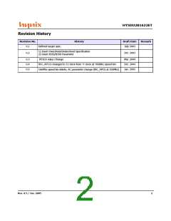
Rev. 0.5 / Jan. 2005
3

 HYNIX [ HYNIX SEMICONDUCTOR ]