HY5DU281622ET
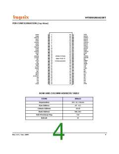
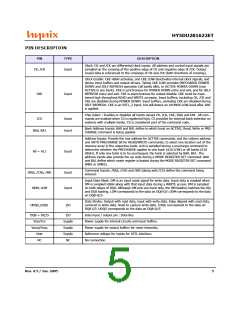
PIN DESCRIPTION
PIN
TYPE
DESCRIPTION
Clock: CK and /CK are differential clock inputs. All address and control input signals are
sampled on the crossing of the positive edge of CK and negative edge of /CK. Output
(read) data is referenced to the crossings of CK and /CK (both directions of crossing).
CK, /CK
Input
Clock Enable: CKE HIGH activates, and CKE LOW deactivates internal clock signals, and
device input buffers and output drivers. Taking CKE LOW provides PRECHARGE POWER
DOWN and SELF REFRESH operation (all banks idle), or ACTIVE POWER DOWN (row
ACTIVE in any bank). CKE is synchronous for POWER DOWN entry and exit, and for SELF
REFRESH entry and exit. CKE is asynchronous for output disable. CKE must be main-
tained high throughout READ and WRITE accesses. Input buffers, excluding CK, /CK and
CKE are disabled during POWER DOWN. Input buffers, excluding CKE are disabled during
SELF REFRESH. CKE is an SSTL_2 input, but will detect an LVCMOS LOW level after Vdd
is applied.
CKE
Input
Chip Select : Enables or disables all inputs except CK, /CK, CKE, DQS and DM. All com-
mands are masked when CS is registered high. CS provides for external bank selection on
systems with multiple banks. CS is considered part of the command code.
/CS
Input
Input
Bank Address Inputs: BA0 and BA1 define to which bank an ACTIVE, Read, Write or PRE-
CHARGE command is being applied.
BA0, BA1
Address Inputs: Provide the row address for ACTIVE commands, and the column address
and AUTO PRECHARGE bit for READ/WRITE commands, to select one location out of the
memory array in the respective bank. A10 is sampled during a precharge command to
determine whether the PRECHARGE applies to one bank (A10 LOW) or all banks (A10
HIGH). If only one bank is to be precharged, the bank is selected by BA0, BA1. The
address inputs also provide the op code during a MODE REGISTER SET command. BA0
and BA1 define which mode register is loaded during the MODE REGISTER SET command
(MRS or EMRS).
A0 ~ A11
Input
Command Inputs: /RAS, /CAS and /WE (along with /CS) define the command being
entered.
/RAS, /CAS, /WE
UDM, LDM
Input
Input
Input Data Mask: DM is an input mask signal for write data. Input data is masked when
DM is sampled HIGH along with that input data during a WRITE access. DM is sampled
on both edges of DQS. Although DM pins are input only, the DM loading matches the DQ
and DQS loading. LDM corresponds to the data on DQ0-Q7; UDM corresponds to the data
on DQ8-Q15
Data Strobe: Output with read data, input with write data. Edge aligned with read data,
centered in write data. Used to capture write data. LDQS corresponds to the data on
DQ0-Q7; UDQS corresponds to the data on DQ8-Q15
U D Q S , L D Q S
I / O
DQ0 ~ DQ15
VDD/VSS
VDDQ/VSSQ
VREF
I/O
Data input / output pin : Data Bus
Supply
Supply
Supply
NC
Power supply for internal circuits and input buffers.
Power supply for output buffers for noise immunity.
Reference voltage for inputs for SSTL interface.
No connection.
NC
Rev. 0.5 / Jan. 2005
5

 HYNIX [ HYNIX SEMICONDUCTOR ]