HY5DU281622ET
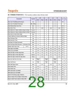
AC CHARACTERISTICS - I (Continued)
4
5
Unit
Note
Parameter
Symbol
Min
15
17
18
10
5
Max
Min
12
13
14
8
Max
Row Cycle Time(Manual Precharge)
Row Cycle Time(Auto Precharge)
Auto Refresh Row Cycle Time
tRC
tRC_APCG
tRFC
-
-
CK
-
-
-
100K
-
-
100K
-
CK
CK
CK
Row Active Time
tRAS
4
Row Address to Column Address Delay for Read
tRCDRD
Row Address to Column Address Delay
for Write
3
-
2
-
tRCDWR
CK
3
1
5
3
2
-
-
-
-
-
2
1
4
3
2
-
-
-
-
-
Row Active to Row Active Delay
Column Address to Column Address Delay
Row Precharge Time
tRRD
tCCD
tRP
CK
CK
CK
CK
CK
Write Recovery Time
tWR
tDRL
Last Data-In to Read Command
Auto Precharge Write Recovery +
Precharge Time
8
-
7
-
tDAL
tCK
CK
ns
4
-
10
-
-
-
CL=4
System Clock Cycle Time
CL=3
5
10
0.45
0.45
-0.6
-0.6
-
0.55
0.55
0.6
0.6
0.4
0.45
0.45
-0.65
-0.55
-
0.55
0.55
0.65
0.55
0.4
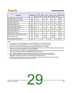
Clock High Level Width
tCH
tCL
CK
CK
ns
ns
ns
Clock Low Level Width
Data-Out edge to Clock edge Skew
DQS-Out edge to Clock edge Skew
DQS-Out edge to Data-Out edge Skew
tAC
tDQSCK
tDQSQ
tHPmin
-tQHS
tHPmin
-tQHS
Data-Out hold time from DQS
Clock Half Period
tQH
tHP
-
-
-
-
ns
ns
1,6
1,5
tCH/L
min
tCH/L
min
Data Hold Skew Factor
Input Setup Time
tQHS
tIS
-
0.4
-
-
0.45
-
ns
ns
6
2
2
0.75
0.75
0.4
0.6
0.6
0.4
0.4
0.72
Input Hold Time
tIH
-
-
ns
Write DQS High Level Width
Write DQS Low Level Width
Clock to First Rising edge of DQS-In
tDQSH
tDQSL
tDQSS
0.6
0.6
1.15
0.6
0.6
1.28
CK
CK
CK
0.4
0.85
Rev. 0.5 / Jan. 2005
30

 HYNIX [ HYNIX SEMICONDUCTOR ]