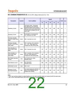
HY5DU281622ET
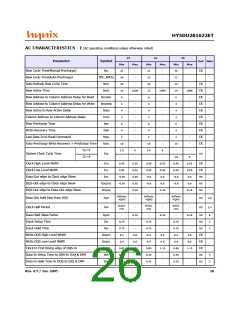
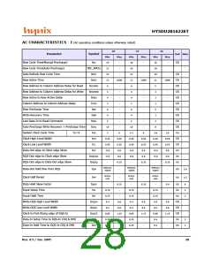
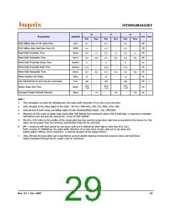
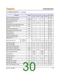
AC CHARACTERISTICS - I (AC operating conditions unless otherwise noted)
25
26
28
Unit Note
Parameter
Symbol
Min
22
24
26
16
6
Max
Min
21
23
25
15
6
Max
Min
20
22
24
14
6
Max
Row Cycle Time(Manual Precharge)
Row Cycle Time(Auto Precharge)
Auto Refresh Row Cycle Time
tRC
tRC_APCG
tRFC
-
-
-
CK
-
-
-
-
-
-
CK
CK
CK
CK
CK
CK
CK
CK
CK
CK
100K
100K
100K
Row Active Time
tRAS
-
-
-
Row Address to Column Address Delay for Read
Row Address to Column Address Delay for Write
Row Active to Row Active Delay
Column Address to Column Address Delay
Row Precharge Time
tRCDRD
tRCDWR
tRRD
4
-
4
-
4
-
4
-
4
-
4
-
2
-
2
-
2
-
tCCD
6
-
-
6
-
-
6
-
-
tRP
4
4
4
Write Recovery Time
tWR
2
-
2
-
2
-
Last Data-In to Read Command
Auto Precharge Write Recovery + Precharge Time
tDRL
10
2.5
-
-
10
2.6
-
-
10
-
-
tDAL
6
6
-
CL=5
System Clock Cycle Time
CL=4
tCK
ns
-
-
2.8
0.45
0.45
-0.6
-0.6
-
6
0.45
0.45
-0.55
-0.55
-
0.55
0.55
0.55
0.55
0.35
0.45
0.45
-0.6
-0.6
-
0.55
0.55
0.6
0.6
0.35
0.55
0.55
0.6
0.6
0.35
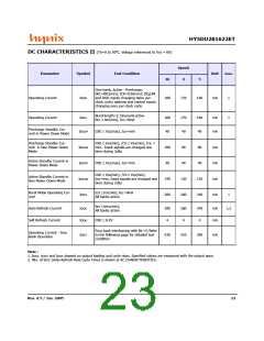
Clock High Level Width
tCH
tCL
CK
CK
ns
ns
ns
Clock Low Level Width
Data-Out edge to Clock edge Skew
DQS-Out edge to Clock edge Skew
DQS-Out edge to Data-Out edge Skew
tAC
tDQSCK
tDQSQ
tHPmin
-tQHS
tHPmin
-tQHS
tHPmin
-tQHS
-
-
-
-
-
-
1,6
1,5
Data-Out hold time from DQS
Clock Half Period
tQH
tHP
ns
ns
tCH/L
min
tCH/L
min
tCH/L
min
-
0.35
-
0.35
-
0.35
6
2
2
Data Hold Skew Factor
tQHS
tIS
ns
ns
ns
CK
CK
CK
ns
ns
0.75
0.75
0.4
-
-
0.75
0.75
0.4
-
-
0.75
0.75
0.4
-
-
Input Setup Time
Input Hold Time
tIH
0.6
0.6
1.15
-
0.6
0.6
1.15
-
0.6
0.6
1.15
-
Write DQS High Level Width
Write DQS Low Level Width
Clock to First Rising edge of DQS-In
Data-In Setup Time to DQS-In (DQ & DM)
Data-In Hold Time to DQS-In (DQ & DM)
tDQSH
tDQSL
tDQSS
tDS
0.4
0.4
0.4
0.85
0.35
0.35
0.85
0.35
0.35
0.85
0.35
0.35
3
3
-
-
-
tDH
Rev. 0.5 / Jan. 2005
26

 HYNIX [ HYNIX SEMICONDUCTOR ]